It's not the first, and won't be the last time in which a 'revolutionary' amplifier just don't live up to it's promises...
Now, to blame it on feedback - how many decently user reviwed amps are there that uses NFB?
There's one here...
http://www.diyaudio.com/forums/showthread.php?postid=679236#post679236
Now, to blame it on feedback - how many decently user reviwed amps are there that uses NFB?
There's one here...
http://www.diyaudio.com/forums/showthread.php?postid=679236#post679236
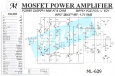
OK...Let's see this schematic
I received it from my friend whom like a several method to apply his NFB schematic.
Notice at R17,C7 it's not feedback point but feedback point is R2...Input Stage...?!?
Does somebody tell me how this method good more than my schematic in first post ?
I still nonplus with this method but I'm designing PCB for it")
PCB comming soon
Regard
AHT
I received it from my friend whom like a several method to apply his NFB schematic.
Notice at R17,C7 it's not feedback point but feedback point is R2...Input Stage...?!?
Does somebody tell me how this method good more than my schematic in first post ?
I still nonplus with this method but I'm designing PCB for it
PCB comming soon
Regard
AHT
Attachments
Hi,
your schematic is a bit unusual in that the signal is connected to the inverting input. The non-inverting input is connected to ground via R17 & C7.
The NFB is quite normal via R4.
What I find really unusual is the omission of a VAS stage to convert the current coming out of the LTP back to a voltage. Instead it is capacitor coupled straight to the drivers. With an RC time constant of 10uS. Where has the treble gone?
I recommend that you move the protection zeners D5 to D8 to the Gate Source leads of the output FETs. In this new location are the diodes D5 & D8 still required? Add back emf protection diodes from each Vrail to output.
R23 & R24 may not be required so just put in a shorting link (do not omit yet).
Finally, how do you intend adjusting output bias current and DC balance? The trimpot seems to be a fine adjust on the LTP tail current used to balance the two halves of the LTP.
Hi,
how can tr11 be first stage of VAS if base is fed from R6?
Tr11 collector goes straight to D3 (no connection to tr13 base).
If I cannot read dots correctly then this just substantiates that the old loops at crossovers was much better ( I still use that when hand drawing).
how can tr11 be first stage of VAS if base is fed from R6?
Tr11 collector goes straight to D3 (no connection to tr13 base).
If I cannot read dots correctly then this just substantiates that the old loops at crossovers was much better ( I still use that when hand drawing).
The base of driver TR13 is connected to collector of TR11. TR5 and TR11 form a VAS Darlington (base of TR11 driven by emitter of TR5). Base of TR5 is connected to collector load R7. Miller Cap C5 from TR11 collector to base of TR5. TR5 functions as a CCS as well with R6 setting current for LTP.
Charles Hansen said:Considered "one of the best" by whom?
So, just what is your problem with Halcro, Charles?
- Status
- This old topic is closed. If you want to reopen this topic, contact a moderator using the "Report Post" button.
- Home
- Amplifiers
- Solid State
- Best driver for MJ15024/25 motorola transistor