Absolutely rigorous analysis as always from you lhquam
The real world measurements may well be only half of what the sims suggest -
but the interesting thing in your simulations are the VERY significant difference in HF impact of the caps in the cascode vs non casc implementations.
What do you think thats attributable to, given the small difference (bw casc and no casc) for the no caps versions ?
Also I have some caps handy that might suit - if you pm me an address, i can drop them in the mail.
My guess is that the significant decrease of THD at high frequencies with cascoding is due to eliminating most of the Miller effect due to the gate-drain capacitance of the drive MOSFET.
What caps did you use? The ones I am planning to order are Nichicon UHW0J153MHD .015 Farad Z=0.010 ohm.
also fwiw, i found that paralleling two low-z caps had better results than one larger cap of equivalent value (due to reduction in esr from leads etc).
Yes, I was guessing that many parallel caps would be better.
My guess is that the significant decrease of THD at high frequencies with cascoding is due to eliminating most of the Miller effect due to the gate-drain capacitance of the drive MOSFET.
I am trying to better understand why the 3rd (odd) harmonics are so greatly reduced at high frequencies by the combination of the caps and cascoding.
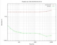
I did a simulation of an unbalanced cascoded configuration with a 4 ohm load. The left plot shown below is a plot of the 3rd harmonic with 1pF and .1F caps. It is nearly identical to the 3rd order plot for the balanced configuration. Of course, with the unbalanced configuration, there is much less even order harmonic cancellation, therefore the THD (not shown) is much higher. This result suggests that the caps with cascoding would be helpful for the unbalanced F5, particularly if the N and P channel MOSFETs are better matched in transconductance and internal Rs.
In the right plot shown below, is a similar simulation for a cascoded F5 circlotron with caps across the source resistors which DOES NOT show a reduction in the 3rd harmonic. I believe that this is due to to topology of the global feedback loops. In the balanced F5, the 2nd harmonics are mostly cancelled by the push-pull outputs before the feedback loop. In the F5 circlotron, each feedback loop receives the output from a single-ended output stage with is highly polluted with 2nd harmonic.
Attachments
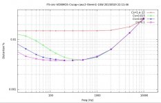
In the right plot shown below, is a similar simulation for a cascoded F5 circlotron with caps across the source resistors which DOES NOT show a reduction in the 3rd harmonic.
The lines in the right chart shows some reductions ? Those are h3 lines right ?
The lines in the right chart shows some reductions ? Those are h3 lines right ?
What I meant to say is that the cascoded circlotron does not exhibit the same behavior at high frequencies as that of the balanced and unbalanced push-pull output stages. Another plot (not shown) shows H3 vs. frequency for an UNCASCODED circlotron with the same values for Cs. That plot is nearly identical to that for the cascoded circlotron. I do not fully understand this result. Clearly something more than the Miller capacitance is involved.
After more simulations and analysis of the circuits, I do not understand why the balanced F5 with output FET cascoding and big caps across the output FET source resistors has such low third (odd) harmonics at high frequencies. Is this a simulation artifact? Can I reproduce this behavior in an actual circuit? 
i read somewhere that caps can screw up THD sim results and the solution is to put a voltage source across each capacitor.
Measure the voltage across each cap in the sim, add correctly polarized voltages across each cap and just set it to the voltages you measured.
Thanks for the suggestion, I will give it a try. I have been very careful in setting up the simulations and making sure that the FFT results are not corrupted, but I am at a loss to explain the high frequency results. They are just too good to believe.
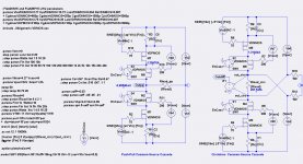
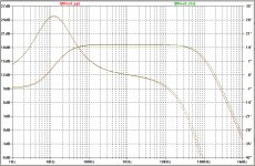
OK, I have clue to what is occurring to cause the 3rd harmonic to be so low with cascoding and caps across the source resistors. Here is a simulation of an F5-style push-pull output stage only, and an F5-style circlotron output stage with and without cascoding. The switches S1-S4 are there to allow the simulation commands to enable or disable the cascode FETs. From left to right the images are the schematic, AC analysis with cascoding, and AC analysis without cascoding. In both plots 0.047F caps were across the source resistors.
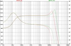
As you can see, with cascoding there is a significant peak in the output stage gain at high frequencies. When global feedback is applied in the full amplifier, this means that there will be a higher feedback factor at higher frequencies, thereby decreasing the harmonic distortion components.
As you can see, with cascoding there is a significant peak in the output stage gain at high frequencies. When global feedback is applied in the full amplifier, this means that there will be a higher feedback factor at higher frequencies, thereby decreasing the harmonic distortion components.
Attachments
Ihq should be congratulated for determining & showing a beautiful example of "asking the right question/s" to ensure the simulator is giving sensible answers.
Don't just accept the first figure, work out what is happening, find how to make sure the simulator is giving one the correct answer to the question being asked.
This methodology confirms earlier advice that beginners that do not understand what they are doing cannot learn by using a simulator. One needs to understand the circuit and how it operates.
I no longer suspect that the simulations are in error. After more simulations and analysis of the cascoded F5 circuit I think I understand why there is a major decrease in the 3rd harmonic at high frequencies. The FQA36P15 PFETs have significantly higher Cgd and Cgs capacitances than the FQA28N15 NFETs. This might contribute enough phase shift difference between the response of the upper and lower F5 feedback loops to result in some 3rd harmonic cancellation at high frequencies.
I need to do some simulations with varying values of the MOSFET Cgs and Cds parameters. This should confirm my suspicions.
I need to do some simulations with varying values of the MOSFET Cgs and Cds parameters. This should confirm my suspicions.
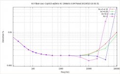
More evidence that the differing MOSFET capacitances and the resulting phase responses are the cause for the "anomalous" low 3rd harmonic at high frequencies as shown in post #138. In the plot below, each MOSFET capacitance of the cascoded, Balanced F5 is multiplied by the parameter Xc. The input JFET capacitances are left alone. With Xc=1, the "nominal" MOSFET Spice model capacitances are used. With Xc=1e-12, the caps are essentially set to zero. As you can see, the "anomalously" low 3rd harmonic is obviously related to the value of Xc.
Attachments
in the models.More evidence that the differing MOSFET capacitances
The sim simply gives the answers to the question you ask.
I am not sure of the point you are making. The simulations provide insights into how the circuit will behave in response to variations in the component parameters, and why some circuit/parameter configurations behave in what appeared to be an "anomalous" manner.in the models.
The sim simply gives the answers to the question you ask.
Is there a was to Piggyback 5 n channel and 5 P-channel mosfets (FQA28N15s and FQA36P15s) into this circuit in respect adding adequate source resistors and it provide more power than the 50 watts usable. I'm wanting a design that will do 250 watts RMS using these transistors, im guessing my question is will the drivers shown drive 10 power transistors without having to modify the circuit shown?
the current design,
the current design, then add more outputs with matching source and gate resistors, (for a total of 5 outputs per rail) or 10 total outputs
clarify idea ;
existing amp complemented with source followers , or just input (Jfet ) core driving multiplied existing outputs ?
the current design, then add more outputs with matching source and gate resistors, (for a total of 5 outputs per rail) or 10 total outputs
- Status
- This old topic is closed. If you want to reopen this topic, contact a moderator using the "Report Post" button.
- Home
- Amplifiers
- Pass Labs
- Balanced F5 in a Small Footprint