It is just a matter of convenience for the open baffle design, but I agree it doesn't really fit in this thread as the B1 has no gain.
Hi guys,
Gain was discussed (at least partially) earlier in the thread. Following advice from Jacques and juma, I am building a version of this circuit with output buffers with gain of 2. In my case there is already a convenient buffer discussed in another thread (http://www.diyaudio.com/forums/pass-labs/146310-bf862-preamp.html) that has a gain of 2, and while I am not competent to post a schematic of a similar idea using 2SK170, there are loads of people who post here (and on this thread, indeed...) who can. With this in mind, would it not be possible for Nelson Bass simply to use such an output buffer on the LP section and leave a passive (unity gain) buffer on the HP??
Cheers
Nigel
Hi Guys,
I'm about to start doing the little DIP-8 and DIP-16 buffer pcbs - all 14 of them, and have a couple of questions before I finalise the design. (I don't want to have to repeat 14 boards because of a stupid mistake... )
)
(I should add, in passing, that the boards in the test preamp I mentioned in #132 are working beautifully, but these are slightly different from the "production" version...)
1. How closely do we need to match Idss on each pair? I've been matching this evening, and while I doubt the absolute accuracy of my measurements I am pretty confident they are good relative to each other. This is because after measuring 20 or so of them, I can go back and check the first ones, and get the same response to within +/- 0.2 %. (I doubted this at first, but after doing 40 or so it seems it is so.) It's a little optimistic to imagine I can get 14 exact matches out of the 60 or 70 jfets I've got on hand, so what do people think? Is +/- 1% good enough? My guess is yes....
2. In juma's preamp circuit there is a 10R resistor on the source of the bottom jfet, and in his symmetrical buffer schematic in post #69 there is one on the top jfet and a trimpot on the lower. In the latter it's pretty clear what these are for - minimising dc offset, although I don't quite understand what it's for in his preamp circuit. It seems it is unnecessary on the buffers here (except the output ones) but I'm a little uncomfortable doing 14 of these buffers without checking I'm not making a stupid mistake.... Right now the plan is to have just the two jfets and their gate resistors on each DIP-8 board.
Cheers
Nigel
I'm about to start doing the little DIP-8 and DIP-16 buffer pcbs - all 14 of them, and have a couple of questions before I finalise the design. (I don't want to have to repeat 14 boards because of a stupid mistake...
)(I should add, in passing, that the boards in the test preamp I mentioned in #132 are working beautifully, but these are slightly different from the "production" version...)
1. How closely do we need to match Idss on each pair? I've been matching this evening, and while I doubt the absolute accuracy of my measurements I am pretty confident they are good relative to each other. This is because after measuring 20 or so of them, I can go back and check the first ones, and get the same response to within +/- 0.2 %. (I doubted this at first, but after doing 40 or so it seems it is so.) It's a little optimistic to imagine I can get 14 exact matches out of the 60 or 70 jfets I've got on hand, so what do people think? Is +/- 1% good enough? My guess is yes....
2. In juma's preamp circuit there is a 10R resistor on the source of the bottom jfet, and in his symmetrical buffer schematic in post #69 there is one on the top jfet and a trimpot on the lower. In the latter it's pretty clear what these are for - minimising dc offset, although I don't quite understand what it's for in his preamp circuit. It seems it is unnecessary on the buffers here (except the output ones) but I'm a little uncomfortable doing 14 of these buffers without checking I'm not making a stupid mistake.... Right now the plan is to have just the two jfets and their gate resistors on each DIP-8 board.
Cheers
Nigel
To set the Id to about 10mA. That's the way I like it - you can do without it (or with anything else you like), you are building it for yourselfHi Guys,
...I don't quite understand what it's for in his preamp circuit....
Hi Guys,
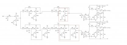
Reading jameshillj's answer I wonder if maybe my post wasn't clear, so let me rephrase. I have posted the circuit I am building, as discussed above in and around post #132, with two red boxes outlined. These are the parts I'm putting on little pcbs, to make building blocks that can be slotted into a p2p motherboard. In fact, the rest of the circuit consists of the filter resistors and caps (which will be on DIP sockets also, but that's a separate issue) and the output buffers, which are done. (In fact, I am redoing them, but again, that's another story). I am not making a pcb for the motherboard. The smaller red box will be a 1cm2 board to slot into a DIP-8 socket, the larger will be DIP-16. So I need 6 of the small ones and 4 of the larger ones. So, let me rephrase my questions.
1. It is easy to match Idss on each jfet pair to with +/- 1% or so. Is there any point to struggling to get better? If I wait for more jfets to arrive I may be able to get to withing +/- 0.2% or so - Is it worth the effort in this case?
2. Is there anything missing in the red boxes in the circuit? During the discussion above juma posted a symmetrical buffer circuit with a 10R resistor on the source of the upper and a trimpot on the lower - clearly to set DC offset. I don't have to worry about DC offset here (caps on output in the end) so the board planned is just jfets and gate resistors. Is there any reason to put a 10R resistor on source(s)? If I understood the earlier discussion then the answer should be no, I would just like to be sure before I do the boards.
jameshillj: Thanks for your answer. You're right about signal and power grounds, but this will be an issue for the p2p layout, not for these little boards. (Actually no ground connection on them at all...)
Cheers
Nigel
Reading jameshillj's answer I wonder if maybe my post wasn't clear, so let me rephrase. I have posted the circuit I am building, as discussed above in and around post #132, with two red boxes outlined. These are the parts I'm putting on little pcbs, to make building blocks that can be slotted into a p2p motherboard. In fact, the rest of the circuit consists of the filter resistors and caps (which will be on DIP sockets also, but that's a separate issue) and the output buffers, which are done. (In fact, I am redoing them, but again, that's another story). I am not making a pcb for the motherboard. The smaller red box will be a 1cm2 board to slot into a DIP-8 socket, the larger will be DIP-16. So I need 6 of the small ones and 4 of the larger ones. So, let me rephrase my questions.
1. It is easy to match Idss on each jfet pair to with +/- 1% or so. Is there any point to struggling to get better? If I wait for more jfets to arrive I may be able to get to withing +/- 0.2% or so - Is it worth the effort in this case?
2. Is there anything missing in the red boxes in the circuit? During the discussion above juma posted a symmetrical buffer circuit with a 10R resistor on the source of the upper and a trimpot on the lower - clearly to set DC offset. I don't have to worry about DC offset here (caps on output in the end) so the board planned is just jfets and gate resistors. Is there any reason to put a 10R resistor on source(s)? If I understood the earlier discussion then the answer should be no, I would just like to be sure before I do the boards.
jameshillj: Thanks for your answer. You're right about signal and power grounds, but this will be an issue for the p2p layout, not for these little boards. (Actually no ground connection on them at all...)
...
Take care to seperate the signal "ground" tracks (filters) from any power rail bipass 0V tracks that you maybe/not use (ie 2 "ground" pins).
... another 2 cents!
Cheers
Nigel
Attachments
Last edited:
To set the Id to about 10mA. That's the way I like it - you can do without it (or with anything else you like), you are building it for yourself
Hi juma,
Our posts crossed... Actually lowering Id a little makes sense to me - for heat reasons if nothing else. A SMD 10R resistor on each source would take very little space on the board, so is quite practical.... I presume It would be better to put one on each jfet to keep things nice and symmetrical, right?
(BTW: I'm redoing the output buffers as DIP-16 boards, as I mentioned in the other thread. I'll post there about them when there's something to say.)
Cheers
Nigel
Hi,
the BF862 without the extra 10r in the source leg operates just like a standard B1. Here the lower FET acts as a CCS and passes a current that is just a bit lower than Idss, due to lower Vds.
The upper FET operates as a source follower (unity gain buffer) and has a bias that equals the CCS. If these two FETs are matched at Idss then the upper FET is biased to between 90% and 100% of Idss.
This will give a consistent performance in all the buffers and will be similar to the way the B1 performs.
If the matching of Idss is not precise then all that happens is that the upper device operates with a bias range that is not quite 90% to 100%. It will be different. If the match were 10% out and the upper FET was the lower Idss of the two then the operating bias would be between 100% and 110%.
If the lower FET were the lower Idss then the upper FET would be biased between 80% and 90%.
You can see that a gross mismatch does not make a lot of difference to the bias of the operating FET. This is because the B1 design is to operate at near Idss.
1% or 2% matching is good enough.
The bigger decisions become selecting an Idss range for all the buffers. Or selecting the higher or lower Idss of the pair for the upper device.
I suspect these two decisions may have an impact on how the whole crossover sounds.
regarding output offset.
The treble side has no problem. the input capacitor blocks DC from every previous stage. there can be no accumulation of offsets.
The bass side is quite different. The final output is DC blocked. That prevents damage downstream. The intermediate stages may suffer from an accumulation of stage offsets. Due to your low rail voltage I suspect that by the time the last stage gets its signal it may be offset so much that a low signal level will suffer excessive distortion or worse, maybe clipping. The offset will certainly reduce the size of undistorted signal that can pass.
I would be very tempted to experiment with a bass channel and measure the variation of offset at the DC blocking capacitor, just to see whether the potential problem needs a "fix" or not.
Hi juma,
....
A SMD 10R resistor on each source would take very little space on the board, so is quite practical.... I presume It would be better to put one on each jfet to keep things nice and symmetrical, right? ...
I posted this earlier, and have been thinking about it some more, and reading back over this and other threads. I think maybe this is wrong, and it would be better to put 10R on the bottom jfet sources, but not on the top.
Here's my reasoning; please help me out correcting anything I've got wrong or misunderstood.
1. The bottom jfet acts a a current sink, so 10R on the source already sets current at the desired point, so there is no need for another on the upper jfet for this reason.
2. DC offset isn't an issue here (since there are output caps at the end of everything) unless the cumulative effects on all buffers must be taken into account. But putting a 10R resistor or not can only make a difference of about 10R*10mA= 0.1V, and the total effect in 3 (HP) or 5 (LP) stages can at worst give 0.5V. In the output buffer the signal immediately before the caps is sitting on about 12V DC, so another 0.5 V or so won't make any realy difference.
3. On the other hand, putting 10R on the sources of the upper jfets sends the signal through at least three SMD resistors for no purpose, which can only make things worse....
So, unless there is some reason not to put 0.5 VDC on the input of juma's preamp, it seems it would be better to put 10R on the lower jfet source, but not the upper jfet.
How's that sound? (And sorry if this is all basic stuff...)
Cheers
Nigel
I'm afraid I can't remember his name but someone posted a link to a paper that described how the set up a dual FET to minimise output offset and using FET temperature characteristics to minimise the drift in output offset.
In this paper he had a source resistor in both the upper and lower FETs.
One lowered the CCS current to where it was near zero tempco.
The upper resistor dropped the output offset to near zero and because it too was running at near zero tempco the drift in output offset was minimal.
All it took was two low value resistors and both were of similar value. I seem to recall <<100r
What you need are the curves of the bf862 that show various Tj and look for the current that minimises tempco. Then run all your FETs at this current. Select the upper resistor to dial out the offset.
Sorry I can't be of more help.
Last edited:
Hi AndrewT,
Again, posts crossed, so I didn't see your first before posting again.
As juma found out, all the jfets I'm measuring fall in a pretty close range, so I'm not going to lose sleep over the range issue. And if I match pairs to within 1% as you suggest then I think this issue is pretty much resolved. I think juma is on the right track reducing Id to 10mA or so, althoguh my main reason is controlling heat on such a small device. (Your and his more technical suggestions are doubtless good reasons also - I'll try to absorb them as best I can...)
It seems to me that the main concern in putting 10R on all the sources is that it would/may introduce noise. But this would principally be a concern on the HP section, right? It may be a good strategy to put 10R only on the CCS jfet in the HP section, relying on the caps following to handle the DC, but to put 10R on *all* sources in the LP section, where cumulative DC may be a problem, but we care less about noise... Sound reasonable?
May be practical, may not be... Have to think about that a bit...
(This was the part I meant when I said I'd have to absorbe this slowly... but that's OK...)
On the contrary, you've been a great help.
Cheers
Nigel
Again, posts crossed, so I didn't see your first before posting again.
...
The bigger decisions become selecting an Idss range for all the buffers. Or selecting the higher or lower Idss of the pair for the upper device.
As juma found out, all the jfets I'm measuring fall in a pretty close range, so I'm not going to lose sleep over the range issue. And if I match pairs to within 1% as you suggest then I think this issue is pretty much resolved. I think juma is on the right track reducing Id to 10mA or so, althoguh my main reason is controlling heat on such a small device. (Your and his more technical suggestions are doubtless good reasons also - I'll try to absorb them as best I can...)
regarding output offset.
The treble side has no problem. the input capacitor blocks DC from every previous stage. there can be no accumulation of offsets.
The bass side is quite different. The final output is DC blocked. That prevents damage downstream. The intermediate stages may suffer from an accumulation of stage offsets. Due to your low rail voltage I suspect that by the time the last stage gets its signal it may be offset so much that a low signal level will suffer excessive distortion or worse, maybe clipping. The offset will certainly reduce the size of undistorted signal that can pass.
It seems to me that the main concern in putting 10R on all the sources is that it would/may introduce noise. But this would principally be a concern on the HP section, right? It may be a good strategy to put 10R only on the CCS jfet in the HP section, relying on the caps following to handle the DC, but to put 10R on *all* sources in the LP section, where cumulative DC may be a problem, but we care less about noise... Sound reasonable?
I would be very tempted to experiment with a bass channel and measure the variation of offset at the DC blocking capacitor, just to see whether the potential problem needs a "fix" or not.
May be practical, may not be... Have to think about that a bit...
I'm afraid I can't remember his name but someone posted a link to a paper that described how the set up a dual FET to minimise output offset and using FET temperature characteristics to minimise the drift in output offset.
In this paper he had a source resistor in both the upper and lower FETs.
One lowered the CCS current to where it was near zero tempco.
The upper resistor dropped the output offset to near zero and because it too was running at near zero tempco the drift in output offset was minimal.
All it took was two low value resistors and both were of similar value. I seem to recall <<100r
What you need are the curves of the bf862 that show various Tj and look for the current that minimises tempco. Then run all your FETs at this current. Select the upper resistor to dial out the offset.
(This was the part I meant when I said I'd have to absorbe this slowly...
but that's OK...)Sorry I can't be of more help.
On the contrary, you've been a great help.
Cheers
Nigel
.... I presume It would be better to put one on each jfet to keep things nice and symmetrical....
Putting 10R in upper JFET Source will increase Zout. DC offset is of no concern because the buffer will be capacitor coupled, but it can be set to zero by means of selecting JFETs by Idss (upper 10-11mA, lower 14-15mA).
Last edited:
this proposal risks biasing the upper FET at greater than it's Idss....it can be set to zero by means of selecting JFETs by Idss (upper 10-11mA, lower 14-15mA).
This could cause a massive increase in gate leakage current and may also give rise to excessive distortion on higher level signals.
Most designers that regularly use jFETs tend to bias them at between 60% and 90% of Idss. Pass' B1 is an exception to this general rule, where it runs at just under Idss. There was one builder of the B1 using selected jFETs that preferred the sound when the slightly lower Idss device was used in the source follower location.
Putting 10R in upper JFET Source will increase Zout. DC offset is of no concern because the buffer will be capacitor coupled, but it can be set to zero by means of selecting JFETs by Idss (upper 10-11mA, lower 14-15mA).
Hi juma,
If I understand correctly, then, you are recommending that I use 10R in the lower jfet and none in the upper jfet. This is what I was speculating might be better in a post after the one you quoted. It also has the KISS advantage ("Keep It Simple, Stupid".)
As a semi-separate issue, you suggest putting a lower Idss jfet above to help reduce the DC offset, but as a practical matter this would be difficult with BF862, since, as you point out elsewhere, they all fall in so close a range when measuring Idss...
I'm afraid the fine points AndrewT raises above are beyond my understanding of electronics, at least at present, but as a practical approach, how about the following:
1. Do the HP section with 10R on the lower jfet source, none on the upper jfet - capacitor at input of each stage eliminates DC without it building up.
2. Try to do the DIP-16 boards for the LP section with a space for a 10R resistor on upper *and* lower jfets, which could be jumpered with a solder bridge. Try it first with 10R on lower jfet, solder bridge on source of upepr jfet; if DC accumulates too badly, put 10R on the upper also, to balance DC a bit....
How does that sound?
Cheers
Nigel
I'm afraid the fine points AndrewT raises above are beyond my understanding of electronics, at least at present, but at this opint I am convinced it is better in the HP section to use just one
...
... this would be difficult with BF862...
Not if you buy 500 pieces as I did
Not if you buy 500 pieces as I did
But didn't you say they all measured very close to each other? In the 100 I bought there certainly wasn't any way to find 14 close to 10mA and 14 close to 14mA - in fact I don't think there was more than 10-15% difference between highest and lowest.... (I have another 100 on the way, so maybe there will be a larger difference between the batches...)
In any event, from what you wrote earlier I think in the HP section just putting 10R on the lower jfet is the way to go, which is a simpler solution if OK. Let the caps deal with the DC offset. In the LP section I suggested earlier putting a space on the board for 10R on both - but use a solder bridge on the upper jfet at first to see if it's OK. If not, put the 10R on. How does that sound?
Cheers
Nigel
But didn't you say they all measured very close to each other? ...
Not all, only about 90%.
You don't need 14+14 odd pieces. The best way to do an ordinary buffer cell is with 2 perfectly matched JFETs.
You want 10+14mA combo just in those buffer cells that will work on higher PS voltage. With +/-9V PS you don't need to worry about Pd.
Hi Jacques Merde, guys,
I am making my PCB for a 2nd order filter based on your schematics (post#14) which has an exclusive buffer for the feedback cap on the low pass section. Since I need to attenuate the LP because my woofers are more sensitive, I put the 20K pot on the direct path after the filter (after C2 and before 220R), but now I fear that the addition of this resistive path to ground could alter the unbuffered LP filter response... and I don't know how to simulate this...should I add a buffer before the attenuator???
Thanks in advance,
M
I am making my PCB for a 2nd order filter based on your schematics (post#14) which has an exclusive buffer for the feedback cap on the low pass section. Since I need to attenuate the LP because my woofers are more sensitive, I put the 20K pot on the direct path after the filter (after C2 and before 220R), but now I fear that the addition of this resistive path to ground could alter the unbuffered LP filter response...
and I don't know how to simulate this...should I add a buffer before the attenuator???Thanks in advance,
M
Hi juma,
I stand corrected. This would give about 50 "outliers", which would probably be enough...
I'm confused here. Except for the output buffers, which follow your BF862 preamp schematic exactly, ALL the buffers will be on +/- 9V, so I don't understand what "higher PSU voltage" means. If I follow your advice to keep around 10mA then I need a source resistor on the CCS jfets, right? So far I am planning on doing this not only for heat reasons, but because my versions of your schematics so far all sound great, which is a pretty strong argument Are you advising against this here?
To try and get a handle on things, let me list options:
1. Match jfets more or less closely. Put 10R (or something) on lower jfet source but not on the upper jfet. This will create a DC offset on the output, but we ignore it. This is probably a good option on the HP, since the caps on the input of the next stage stop the DC. May need to alter this idea on the LP.
2. Deliberately choose unmatched jfets so Idss of the upper one is equal (or close to) the Ids the CCS produces with the 10R in place, and hence eliminate (or nearly) the DC offset.
3. Match jfets as closely as possible and put no source resistors anywhere, and run the whole thing at Idss. (I would probably like to redo the pcb test if this is the preferred option, but that isn't a big deal......)
1 and 3 can be tried and changed, possibly, using either jumpers or resistors on the boards. 2 can't be tried and changed so easily... Of course, I can mix this around a bit. Maybe best is 1 on the HP and 2 on the LP, or something.... I suppose the real issue is deciding what Id should be... since your schematics sound good at 10mA that's a good reason for putting 10R on the source, I guess...? Any thoughts?
Cheers
Nigel
Not all, only about 90%.
I stand corrected. This would give about 50 "outliers", which would probably be enough...
You don't need 14+14 odd pieces. The best way to do an ordinary buffer cell is with 2 perfectly matched JFETs.
You want 10+14mA combo just in those buffer cells that will work on higher PS voltage. With +/-9V PS you don't need to worry about Pd.
I'm confused here. Except for the output buffers, which follow your BF862 preamp schematic exactly, ALL the buffers will be on +/- 9V, so I don't understand what "higher PSU voltage" means. If I follow your advice to keep around 10mA then I need a source resistor on the CCS jfets, right? So far I am planning on doing this not only for heat reasons, but because my versions of your schematics so far all sound great, which is a pretty strong argument
Are you advising against this here? To try and get a handle on things, let me list options:
1. Match jfets more or less closely. Put 10R (or something) on lower jfet source but not on the upper jfet. This will create a DC offset on the output, but we ignore it. This is probably a good option on the HP, since the caps on the input of the next stage stop the DC. May need to alter this idea on the LP.
2. Deliberately choose unmatched jfets so Idss of the upper one is equal (or close to) the Ids the CCS produces with the 10R in place, and hence eliminate (or nearly) the DC offset.
3. Match jfets as closely as possible and put no source resistors anywhere, and run the whole thing at Idss. (I would probably like to redo the pcb test if this is the preferred option, but that isn't a big deal......)
1 and 3 can be tried and changed, possibly, using either jumpers or resistors on the boards. 2 can't be tried and changed so easily... Of course, I can mix this around a bit. Maybe best is 1 on the HP and 2 on the LP, or something.... I suppose the real issue is deciding what Id should be... since your schematics sound good at 10mA that's a good reason for putting 10R on the source, I guess...? Any thoughts?
Cheers
Nigel
- Status
- This old topic is closed. If you want to reopen this topic, contact a moderator using the "Report Post" button.
- Home
- Amplifiers
- Pass Labs
- B1 Active Crossover