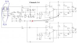
I tried not to change anything, so I connected JP2 1&2 and JP2 9&10 to the +/- of the RCA inputs.
I cut the resistor to take out the mute circuit from Pin 8 and added a 10k resistor from the pad gong to Pin 8 and soldered it to the leg of C30 (0.12uF) going to Pin 4.
I connected all the grond leads back to the "star Ground" on a bolt attached to the bottom of the case. It has about 12 leads attached to this one bolt.
I have not touched/altered anything about the grounding scheme.
Here is a very bad drawing of what I have done, for a graphic description.
Attachments
I did remove R48, and use the pad that goes to PIN 8 for one side of the 10k resistor and then went to the 0.12uF Cap (C30) as a point to connect to PIN 4.
Ok I checked again - and the schematic isn't 100% accurate.
R63 is a jumper wire, but R62 is a 0.1uF film capacitor.
The other Channels (1-2, 5-6) have R60, R64 as open and R61, R65 with jumper wires.
Obviously this board/power supply combo were used in multiple amplifiers, so has some varioations to the schematic I posted.
- Status
- This old topic is closed. If you want to reopen this topic, contact a moderator using the "Report Post" button.