It is true that IR2110 are tricky to use. I have a long experience using them in Class-D amplifiers (have a look at "Mosfet reliability in Class-D amplifiers" thread, or something like that, under "Class-D" forum).
First, a lot of mosfets blew up instantaneously just like in this supply, with no apparent reason. I rearranged the layout paying great attention to the gate loop and used more rugged mosfets (moved from OnSemi to IRF) and since them I have had no problems, and I have tested them quite a bit!
All that experience has been applied here, so my layout, at least in that respects to the IR2110 chip and gates should be ok. Anyway, I was cautious enough to add a double footprint in order to add a gate drive transformer in the same board, that I will test soon (I am fed up with so much mosfet and drivers changes!)
This way even the SG3525 chip seems to have died.
If the problem was excessive Vgs voltage due to resonance, what about adding 15V zeners in parallel with Vgs? I know they are not recommended for high frequency, but at 80 KHz...
But if it is due to spurious turn on causing shoot-through, that's a different story...
BTW: Danko, my bootstrap capacitor is 10uF, should be enough. Gate resistors are now 15 ohm.
I have changed the IR2110 to a SD250-4 Coilcraft gate-drive transformer. I still haven't soldered my mosfets, but with 1nF capacitor load, the Vgs waveform looks clean (bipolar, +/-15V amplitude, and a rise time from 0 to 15V of around 350nS, I assume that this will produce much faster rise time in the mosfets, as the Vth level is reached in around 50-80ns)
My mosfets are rated at +/-30v Vgs voltage, so they shouldn't be damaged by the +/-15V bipolar wavefrom... I will cross my fingers.
This afternoon I will test all and tell you how it goes. At least I won't have to change my chips once a day during my testing phase.
Pierre.
My mosfets are rated at +/-30v Vgs voltage, so they shouldn't be damaged by the +/-15V bipolar wavefrom... I will cross my fingers.
This afternoon I will test all and tell you how it goes. At least I won't have to change my chips once a day during my testing phase.
Pierre.
More about my progress....
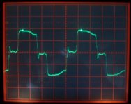
I exchanged the IR2110 by a GDT (Coilcraft sd250-4). The figure shows the waveform of Vgs. It is clean although a bit slow for my taste, and there are a peak that may trigger the mosfet (although the other will be off so I don't think that's an issue).
I have been able to obtain 375W with this and observe a good switching waveform. I haven't tried more but I am sure it will do well. I am almost sure that the mosfets heat up more quickly than with the IR2110 driver, I suppose that the rise/fall times are slower, so
I will try to add a NPN/PNP buffer for the SG3525 to speed up things a bit.
I have finally decreased sw. freq. to 40KHz, and now they become less hot, so switching losses must be dominating.
Unfortunately, when I have soldered the transformer and everything ok, I have done an stupid mistake and something has exploded and broken (but not the mosfets) But as soon as I have repaired all, I will try to add regulation.
Attachments

Yes, the SG3525 doesn't have a whole lot of drive current available, so rise times are slower than what you'd like because it takes longer to get charge to the gates. The IR part has 2 amps available for each device compared to 400mA for the SG part. I think your results will be much better after adding the additional driver circuitry.
Matt.
Matt.
The transformer gate drive waveform shows that the transformer is saturating and that leakage inductance is already limiting MOSFET turn-off speed, so it can't be improved. There may be also some cross conduction due to the leakage inductance spike.
You can't just drive MOSFET gates directly from a transformer and expect low losses, this only works with IGBTs that have input capacitances almost an order of magnitude lower than MOSFETs, and with bipolar transistors that are current driven.
It would be a good idea to add some kind of gate buffering, at least for turn-off. Don't try to load the transformer with a lower gate resistor to get faster turn-off since this will only make the leakage inductance spike issue worse.
Eva, you are right in that last affirmation: I already tried to lower the gate resistor. Now is 15 ohm but I tried up to 0 ohm, and yes, it switches a bit faster but the spike rises, so I didn't try with the mains switched on for security.
So, from what you are saying, if I keep the mosfets, I should look for another transformer, right? Can you suggest any commercial model that could work, having a look at the specifications of SD250-4?
Thanks!
So, from what you are saying, if I keep the mosfets, I should look for another transformer, right? Can you suggest any commercial model that could work, having a look at the specifications of SD250-4?
Thanks!
mmmm.
Have been thinking about the GDT a little bit more. Eva, how do you know that it is saturated?
It is rated at 375V-us, so as I drive it in a bipolar fashion, (+/-12V), at 40 or even 80 KHz, there shouldn't be any problem, right?
If it is still usable at that frequency, how can I speed it up to minimize losses?
Another question: can I simply substitute the mosfets by IGBTs (properly rated and fast enough for that frequency, of course)?
Thanks!
Pierre said:mmmm.
Have been thinking about the GDT a little bit more. Eva, how do you know that it is saturated?
It is rated at 375V-us, so as I drive it in a bipolar fashion, (+/-12V), at 40 or even 80 KHz, there shouldn't be any problem, right?
If it is still usable at that frequency, how can I speed it up to minimize losses?
Another question: can I simply substitute the mosfets by IGBTs (properly rated and fast enough for that frequency, of course)?
Thanks!
From drooping dc level on your gate pulses. 10 different choices also why it is happening, I dont know your exact part values and scematics so difficult to say. Do you use dc-decoupling cap on GDT primary? too small dc-decoupling cap or too small chip vcc cap can cause similar dc pulse drooping as core saturation.
I dont see any tricks to speed it up, lower leakage tranny is only option if your layout is already reasonablyy good. I have had good results with DIY gate drive toroids, sub 50ns risetimes to 6nF load with minimal ringing. Sorry, cant recommend any off-the-self products.
The thing is that, the more I look at the specifications of the SD250-4 transformer I am using, the more convinced I am that it is perfectly suitable and that it should produce much better results.
It has relatively low primary inductance: 1.5mH and leakage inductance (4 uH max), 375 V-us ET product (fast enough), specified for 10-250KHz use, I am at 40 or 80 KHz... Why should it be saturating?
I am driving it in a bipolar fashion directly from the SG2525 chip, with a 4.7 ohm resistor in series with the primary (no coupling cap), and 15 ohm resistor in series with each gate.
And the mosfets are not specially slow: 52nC max gate charge, 1400pF max input capacitance.
The tracks are quite short. Am I doing something wrong?
MOSFET turn-off is a delicate process because a 300V positive-going pulse is coupled to the gate through reverse transfer capacitance. That's why driving MOSFETs from transformers produces high losses and sometimes cross-conduction.
The usual approach is to use a PNP emitter follower and some additional components to buffer turn-off process. Leakage inductance is quite hard to reduce, and it increases with volts*seconds product rating.
Also, IGBTs will be a direct replacement for MOSFETs and they will actually switch faster with the same transformer and gate resistors because their capacitances are an order of magnitude lower.
You may also try to solve the gate drive IC issue. If it's a gate overvoltage issue, Zeners and schottkys soldered directly across gate and source terminals may solve the problem.
Could you show us your schematic and layout? There may be some non obvious mistake that you are overlooking.
Hello, Eva. Nice to hear from you again.
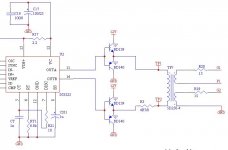
Here is my drive stage schematics. Forget the NPN/PNP buffer because it is not implemented by the moment, although I would like to try it at some moment. I have ordered a couple of samples of Pulse GDT's, let's see if they work better.
I have selected this IGBT, do you think it can be suitable for 40 to 80KHz operation? : IRG4BC20W
Attachments
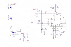
Now I have another problem: I am trying to implement regulation, using an optocoupler (see attached schematics).
The problem is that, while adjusting the potentiometer, R16, (that does vary the "ERROR" node voltage from 0 to around 9V), it cannot make the PWM go lower than maximum duty-cycle, that is, the output of the error amplifier inside the SG3525 chip doesn't go lower than about 3.7v (max. duty cycle corresponds to about 3.5v).
In fact, I have tested with no power, simulating the NFB loop by putting a variable voltage at the "ERROR" node, and as I increase it, the error amp. output goes down to about 3.7V and there is a point where it starts going up again, so I can never reach PWM less than around 50%. Strange, isn't it?
I think it is an issue with the reference applied to NI input or something like that.
Best regards,
Sergio
Attachments
IGBTs don't have a body diode like MOSFETs so you should either solder a diode between collector and emitter or get an IGBT with built-in diode.
IRG4BC20W doesn't include a clamping diode but otherwise it would be fine. Note that reverse transfer capacitance is less than 10pF. Also note that IGBT conduction losses at low currents will be higher than in MOSFET, but they won't skyrocket as current is increased like in MOSFETs.
IRG4BC20W doesn't include a clamping diode but otherwise it would be fine. Note that reverse transfer capacitance is less than 10pF. Also note that IGBT conduction losses at low currents will be higher than in MOSFET, but they won't skyrocket as current is increased like in MOSFETs.
Yes, Eva, they seem good enough and not very expensive. Thanks.
About regulation, I have built a small prototype board with the sg3525 chip just for testing, and found that the problem was that the inverting input gain (resistor between pins 1 and 9) was too low: 1.5 V/V (R was 15k and input R was 10k), so the error opamp output (pin 9) was doing strange things (as not inverting for some input ranges).
Once I have increased that resistor to >150K (G>15), the circuit responds linearly with increasing duty cycle for decreasing voltage and vice-versa. All this in a very limited range of about 300mV of input voltage around 5.1v (Vref): Below around 4.95V, PWM is 47%, and above around 5.25V, PWM is 0%.
I will try to make the modification in my SMPS and test if it regulates correctly.
Best regards,
Pierre
SG3525A suffers from error amplifier latching when inputs are allowed to go below 1V above groud or so. I stumbled into similar problem because I'm using this error amplifier for average current control, and I solved it by adding a 2.5V bias to both signals.
There are other low-cost ICs like TL494 whose common mode input range includes ground, but TL494 has its own drawbacks in comparison with SG3525, particularly it lacks double pulse supression and premature pulse termination capabilities.
Also, be very careful when loading COMP output of SG3525A, it has a very low sink current capability, something like 100uA, so load impedances below 50K may be troublesome. Try to use that amplifier as an unity gain buffer and place the actual error amplifier and its compensation in the secondary side instead, before the optocoupler.
Ok, thanks for the suggestions.
As a first approach, I will use the SG3525 error amplifier in the primary side and only zeners+resistors in the secondary, as shown in the schematics I posted. Let's see how it works then. Once it is up and running, I will try to improve it.
As for the coupled inductor to balance both outputs, I am planning to stack two T106-2 cores (micrometals) and bifilar wind about 40 turns for 20uH, with 1mm wire. Then I will use one wire for each rail, but in opposite directions.
Hope this work well for the kind of power I am trying to achieve.
Best regards,
Pierre
- Status
- This old topic is closed. If you want to reopen this topic, contact a moderator using the "Report Post" button.
- Home
- Amplifiers
- Power Supplies
- Assymmetric outputs in half-bridge