Hi eLarson,
Thank you for the encouragement. I'm posting an updated schematic. I've inserted a gain setting resistor between the gain Q sources. In the "Zen Variations 6" article NP states that the SOZ shown has a gain of 12dB. This translates to a gain of 4. With an output impedance of 16 the total Q source resistance is 4. Subtracting the 1 ohm resistor and dividing by 2 gives an apparent source resistance of 1.5 ohms for each IRFP240 at this voltage and current (3A). The F1 has a gain of 14dB or 5 which when divided into the 80 ohm output impedance of the F1 means there is a required total Q source resistance of 16 ohms. The current in my amp is only .9A or so but I think that a 12 ohm gain setting resistor between the sources is good ballpark choice for a gain of about 14dB.
I will return when I've turned it on and played with it.
Graeme
Attachments
gl´s circuit
Hello,
in difference to your circuit the F1 is working from a single supply and a single current source to ground.
Therefore there must be resistive voltage dividers to the gates of the amplifying fets and dc blocking input caps.
Reinhard
See attache file, 5 Fets per channel
Hello,
in difference to your circuit the F1 is working from a single supply and a single current source to ground.
Therefore there must be resistive voltage dividers to the gates of the amplifying fets and dc blocking input caps.
Reinhard
See attache file, 5 Fets per channel
Attachments
Hello Reinhard,
Thank you for the photo and for your comments. The photo confirms that the actual F1 circuit is close to the functional diagram in the manual and is indeed close to the SOZ as NP has already stated. I chose to use dual supplies and also to break the lower CCS into 2 parts because I intend to add an Aleph-X front end onto the circuit as a next step. This will also completely change the way the gain is set.
I agree with your comment abouts about the resistor dividers on the gates and the coupling capacitiors. It seems like they must be there if the F1 is operating off a single supply.
Graeme
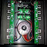
moe29 said:where did the picture of the F1 come from?
It looks like the one here:
http://www.6moons.com/audioreviews/audioreviews.html
I had decided that my experimental transconductance amp did not have the proper output impedance. The upper CCS's have much too high an impedance on their own. I was going to drop a 56 ohm 3W resistor (oo magic - I just have a big bag of them) to ground from each of the drains of the gain Q's in a manner similar to the Aleph P. However NP has just dropped a major hint on a thread over in loudspeakers.
So I have adjusted my schematic. Comments?
Graeme
The F1 has an intrinisc output impedance of about 1 K ohm,
and I parallel 94 ohms across the output to establish about
80 ohms output impedance.
So I have adjusted my schematic. Comments?
Graeme
Attachments
Hi eL,
Ideal is ideal. But in this case we want a finite gain which demands finite values for such parameters as output impedance. NP chose 80 ohms for the F1 and I simply used that as a general target.
I have stated in earlier posts that this piece is under construction. I have not yet listened to it. These discussions have definitely helped to move the design in the right direction and I very much appreciate your input.
Graeme
Re: 2-way
There becomes a need to completely rework the XO (Nelson talks about putting compenents in shunt instead of series... best to use 2 1st watts & an active XO :^)
dave
MikeW said:How does the first watt amp sound with 2-way speakers?
There becomes a need to completely rework the XO (Nelson talks about putting compenents in shunt instead of series... best to use 2 1st watts & an active XO :^)
dave
Re: gl´s circuit
Hi
This is my first post to this forum
so please be gentle with me.
I took a look at the circuit posted by gl.
I have a few comments, suggestions, please
take them or leave them as you see fit.
1. You are using split voltage supplies but
the input of the amp as far as I can see is
biased to ground. The back to back zeners on
the input are presumably for clamping the input
swing. This means your single ended output
voltage swing is going to be limited to roughly
Vgs - Vdsat of the input transistor plus
Vsupply - Vdsat of the upper current mirror minus
the voltage drop across the 0.75 ohm resistor.
This gives you a theoretical maximum voltage
swing of something much under 20V. This for a
dual supply design. Obviously the differential
swing will be double this.
Looking at the IRFP240 and IRFP9240 datasheets,
it is impossible to tell where the devices will
bias up with 1 amp current.
BTW using these power MOSFETs maybe a significant
overdesign, they can handle much more power
than you can ever get out of the circuit. Plus
the datasheet gives not much useful information
for the current you are operating at !
Your quiescent power dissipation will be something
of the order of 20W (Vds*Ids) max per transistor.
Maybe take 40W to be on the safe side.
The Pchannel device has lower output impedance
than the nChannel, you may want to consider
cascoding the upper current mirrors, but this will
eat into you available voltage output swing but
if done with care will further improve your PSRR
and output linearity.
The back to back zeners on the input are probably
unecessary for a transconductance amp since the
output current will be limited, at least in theory,
by the current available from the current sources.
2. Without some form of common mode
feedback it will be real tricky to trim
the 4 current sources to get the output biased
up correctly. If you leave the input biased
at ground you will want to bias the output at
around 10V to get symetric output swings. You
can modify the common mode circuit from the
Zen Variations 7 article to achieve this.
Though there are many ways you could do this.
If you are planning on leaving the 2 47ohm
resistors in the circuit you can use their
common point to sense the dc output voltage.
3. Coming back to the limited potential voltage
swing from the dual voltage supplies. You can use
the -20 volts that really serves no useful
purpose here to improve the noise floor. By
using a single current source on the bottom and
splitting the degeneration resistor in 2. Like
this the noise from the lower nChannel current
source will be rejected (at least theoretically
to a first order) by the differential output.
1 amp through 6ohms gives 6 volts (I know !)
which still leaves a chunk of spare voltage
across the lower nChannel current source.
Your degeneration values should make the input
as linear as a very linear thing !
Or you can keep it as is and drop the input
bias voltage level thereby gaining more
voltage swing and use an ac coupling capacitor.
Since you have the headroom cascoding this
guy won't do any harm either and will improve
the PSRR and linearity of the amp, particularly
it's even order linearity.
4. Your current source scheme seems reasonable,
seems to give a -ve temp co, falling current
with increasing temperature, don't forget to
mount the npn's on the heatsink along with the
power devices.
You have potentially a lot of gain in the feedback
loop depending on the current running through
the npn. The miller cap uses this gain to your
advantage and should help with PSRR.
There you go, hope some of this stuff was useful.
Again take it or leave it as you wish.")
herisson
Hi
This is my first post to this forum
so please be gentle with me.
I took a look at the circuit posted by gl.
I have a few comments, suggestions, please
take them or leave them as you see fit.
1. You are using split voltage supplies but
the input of the amp as far as I can see is
biased to ground. The back to back zeners on
the input are presumably for clamping the input
swing. This means your single ended output
voltage swing is going to be limited to roughly
Vgs - Vdsat of the input transistor plus
Vsupply - Vdsat of the upper current mirror minus
the voltage drop across the 0.75 ohm resistor.
This gives you a theoretical maximum voltage
swing of something much under 20V. This for a
dual supply design. Obviously the differential
swing will be double this.
Looking at the IRFP240 and IRFP9240 datasheets,
it is impossible to tell where the devices will
bias up with 1 amp current.
BTW using these power MOSFETs maybe a significant
overdesign, they can handle much more power
than you can ever get out of the circuit. Plus
the datasheet gives not much useful information
for the current you are operating at !
Your quiescent power dissipation will be something
of the order of 20W (Vds*Ids) max per transistor.
Maybe take 40W to be on the safe side.
The Pchannel device has lower output impedance
than the nChannel, you may want to consider
cascoding the upper current mirrors, but this will
eat into you available voltage output swing but
if done with care will further improve your PSRR
and output linearity.
The back to back zeners on the input are probably
unecessary for a transconductance amp since the
output current will be limited, at least in theory,
by the current available from the current sources.
2. Without some form of common mode
feedback it will be real tricky to trim
the 4 current sources to get the output biased
up correctly. If you leave the input biased
at ground you will want to bias the output at
around 10V to get symetric output swings. You
can modify the common mode circuit from the
Zen Variations 7 article to achieve this.
Though there are many ways you could do this.
If you are planning on leaving the 2 47ohm
resistors in the circuit you can use their
common point to sense the dc output voltage.
3. Coming back to the limited potential voltage
swing from the dual voltage supplies. You can use
the -20 volts that really serves no useful
purpose here to improve the noise floor. By
using a single current source on the bottom and
splitting the degeneration resistor in 2. Like
this the noise from the lower nChannel current
source will be rejected (at least theoretically
to a first order) by the differential output.
1 amp through 6ohms gives 6 volts (I know !)
which still leaves a chunk of spare voltage
across the lower nChannel current source.
Your degeneration values should make the input
as linear as a very linear thing !
Or you can keep it as is and drop the input
bias voltage level thereby gaining more
voltage swing and use an ac coupling capacitor.
Since you have the headroom cascoding this
guy won't do any harm either and will improve
the PSRR and linearity of the amp, particularly
it's even order linearity.
4. Your current source scheme seems reasonable,
seems to give a -ve temp co, falling current
with increasing temperature, don't forget to
mount the npn's on the heatsink along with the
power devices.
You have potentially a lot of gain in the feedback
loop depending on the current running through
the npn. The miller cap uses this gain to your
advantage and should help with PSRR.
There you go, hope some of this stuff was useful.
Again take it or leave it as you wish.
herisson
Hi herrison,
Welcome to this forum and thank you for your detailed and very thoughtful critique of the G1 circuit. Your remarks are very encouraging.
I would like to start by saying that I agree with all of your analysis and suggestions. Please note that I am still building this circuit. It is not yet tested.
1) The amplifier is modeled after the Son of Zen, hence the ground reference. I also wanted to avoid input coupling caps. The zeners are protection against static discharge from human hands on the input connections. My listening room is carpeted. The mosfets were chosen because I already own them. I consider 20W to be a good number. You are right 40W is OK but it is too high a dissipation for my heatsinks without forced air. I agree with your comments on cascoding, but I wanted to keep this first version simple. I will add your ideas to my list of things to try.
2) I agree with you here too. My greatest concern is stability; both from oscillation and drift. Your suggestion about using the center point of the 47 ohm resistors to provide a reference in the manner of the Zen V7 is thought provoking. This may be what NP has done in the F1.
3) Again I agree with all of your comments. Shouldn't the 12 ohm resistor betweeen the sources have the same linearizing effect as your two 6 ohm resistors?
I am a big fan of cascoding. I have wondered if cascoding the gain transistors would counteract the Vgs non-linearity. Is this what you are suggesting?
4) I am not certain I agree with your suggestion about putting the CCS BJT's in contact with the heatsinks. The BJT needs to be a fixed voltage reference Vbe) across the mosfet source resistor. Assuming the resistor value doesn't drift due to heating then all should be well.
Thank you again for your comments and encouragment.
Graeme
gl said:I agree with you here too. My greatest concern is stability; both from oscillation and drift. Your suggestion about using the center point of the 47 ohm resistors to provide a reference in the manner of the Zen V7 is thought provoking. This may be what NP has done in the F1.
I did leave some bread crumbs on the trail.
hi graeme
You could think about just adding 2 back to back
directly across the inputs to simplify the design
a bit more.
I guess from Mr. Pass's comment he would appear
to think this should work without oscillating !
The common mode feedback should also take care of
some of this temperature drift. If you use the 47
ohm resistors instead of the 27k in the zen v7 your
common mode feedback loop will have less gain anyway
and should be more stable.
Yes and not quite. I was thinking the split
scheme may reduce even order distortion but
I have no hard evidence to back this up.
You already have the headroom for free,
a single source will be easier and cheaper to
build plus you get the added benefit of less noise
in theory. It's normally a headroom against
noise trade-off.
No, cascoding the gain transistors should have no
impact on the Vgs non-linearity, with your design
you have already reduced some of this nonlinearity
with the negative feedback from the degeneration.
Cascoding the gain transistors and the upper current
sources will increase their output impedance and
should mean you can swing a larger output voltage
for a given distortion. BUT without changing the bias
point the overall maximum potential voltage swing
will be lower than without the cascode.
You're right, I was thinking that the BJT needed
to be at the same temperature as the MOS in order to
give a -ve tempco. If the temperature of the BJT
remains relatively constant the temp co. of the resistor
will set the overall current temp co.
Another comment and you may already know this, but
these differential designs always look great on
paper, the way they are built however will have a big
influence on the performance. Matching is highly
critical, the better the matching you can achieve
the better the overall performance.
Again hope this helps.
BTW: I have a modified schematic of your amp showing
the ideas but it's in .tif format ! I'll see if I can translate
it to something I can post.
1) The amplifier is modeled after the Son of Zen, hence the ground reference. I also wanted to avoid input coupling caps. The zeners are protection against static discharge from human hands on the input connections. My listening room is carpeted.
You could think about just adding 2 back to back
directly across the inputs to simplify the design
a bit more.
2) I agree with you here too. My greatest concern
is stability; both from oscillation and drift.
Your suggestion about using the center point of
the 47 ohm resistors to provide a reference in
the manner of the Zen V7 is thought provoking.
This may be what NP has done in the F1
I guess from Mr. Pass's comment he would appear
to think this should work without oscillating !
The common mode feedback should also take care of
some of this temperature drift. If you use the 47
ohm resistors instead of the 27k in the zen v7 your
common mode feedback loop will have less gain anyway
and should be more stable.
3) Again I agree with all of your comments.
Shouldn't the 12 ohm resistor between the
sources have the same linearizing effect
as your two 6 ohm resistors?
Yes and not quite. I was thinking the split
scheme may reduce even order distortion but
I have no hard evidence to back this up.
You already have the headroom for free,
a single source will be easier and cheaper to
build plus you get the added benefit of less noise
in theory. It's normally a headroom against
noise trade-off.
I am a big fan of cascoding.
I have wondered if cascoding the gain
transistors would counteract the Vgs
non-linearity. Is this what you are suggesting?
No, cascoding the gain transistors should have no
impact on the Vgs non-linearity, with your design
you have already reduced some of this nonlinearity
with the negative feedback from the degeneration.
Cascoding the gain transistors and the upper current
sources will increase their output impedance and
should mean you can swing a larger output voltage
for a given distortion. BUT without changing the bias
point the overall maximum potential voltage swing
will be lower than without the cascode.
4) I am not certain I agree with your
suggestion about putting the CCS BJT's in contact
with the heatsinks. The BJT needs to be a fixed
voltage reference Vbe) across the mosfet source resistor.
Assuming the resistor value doesn't drift due to heating
then all should be well.
You're right, I was thinking that the BJT needed
to be at the same temperature as the MOS in order to
give a -ve tempco. If the temperature of the BJT
remains relatively constant the temp co. of the resistor
will set the overall current temp co.
Another comment and you may already know this, but
these differential designs always look great on
paper, the way they are built however will have a big
influence on the performance. Matching is highly
critical, the better the matching you can achieve
the better the overall performance.
Again hope this helps.
BTW: I have a modified schematic of your amp showing
the ideas but it's in .tif format ! I'll see if I can translate
it to something I can post.
Hi herisson,
Thank you again for your further comments.
Thank you for the comment on the cascoding and Vgs linearization.
My gain mosfets are matched to within 10mv at an Id of 500ma. So are the CCS mosfets although I don't believe they need to be. I had a number of spare matched pairs available so I used them.
I agree with you, a single CCS on the -ve side such as in the Zen V7 is simpler and more elegant if all you want to build is just a transconductance SOZ. However, I chose to use separate CCS's on the gain Q sources because I would like to add a front end diff pair in an X type circuit. The separate CCS's make the design physically and thermally more convenient to build. It is interesting, I have found examples of 2 stage transconductance amplifiers on the web that are designed as one diff pair nested within another. These were found in papers on IC design. Again, all very thought provoking. You have made me re-think my -ve CCS design.
I look forward to seeing your schematic.
Mr. Pass has been most gracious with his bread crumbs. Until all 100 of those nifty F1's are sold we all need to gracious as well. After all, the more bread he makes the more crumbs he can spread. (I'm sorry - I couldn't resist).
Thank you.
Graeme
Hi Graeme,
Actually I had another think about this and revised my position:
because of the negative feedback you have in place at
least for small input signals the effect of the mismatch on
distortion and noise should be minimised.
Another thing I just realised is that with an 8ohm load your
amp will have a voltage gain of a little over 5 dB.
You may want to consider backing off your degeneration by
6dB otherwise you're going to have drive the amp harder.
Would it be possible for you to post the schematic for the final
circuit you have in mind? I can't really visualise what you are
intending to do.
I agree.
I think I have some idea of the type of circuit you are refering to, can you
post the link ? If it's what I'm thinking you will end up with something
that embodies the principals of the "X circuit": differential output plus
degeneration plus a negative overall feeback loop !
oh, nearly forget the schematic, here you go.
My gain mosfets are matched to within 10mv at an Id of 500ma.
So are the CCS mosfets although I don't believe they need to
be. I had a number of spare matched pairs available so I used them.
Actually I had another think about this and revised my position:
because of the negative feedback you have in place at
least for small input signals the effect of the mismatch on
distortion and noise should be minimised.
Another thing I just realised is that with an 8ohm load your
amp will have a voltage gain of a little over 5 dB.
You may want to consider backing off your degeneration by
6dB otherwise you're going to have drive the amp harder.
I agree with you, a single CCS on the -ve side such as in the
Zen V7 is simpler and more elegant if all you want to build is
just a transconductance SOZ. However, I chose to use separate
CCS's on the gain Q sources because I would like to add a front
end diff pair in an X type circuit.
Would it be possible for you to post the schematic for the final
circuit you have in mind? I can't really visualise what you are
intending to do.
The separate CCS's make the design physically and thermally
more convenient to build.
I agree.
It is interesting, I have found examples of 2 stage transconductance
amplifiers on the web that are designed as one diff pair nested within
another.
I think I have some idea of the type of circuit you are refering to, can you
post the link ? If it's what I'm thinking you will end up with something
that embodies the principals of the "X circuit": differential output plus
degeneration plus a negative overall feeback loop !
oh, nearly forget the schematic, here you go.
Attachments
Hi herisson,
Your comment about the voltage gain is correct. However, this is a transconductance amplifier. It is the output current as a function of input voltage that's important. In NP's article on current amplifiers and high efficiency speakers you'll note that the EQ network reduces the voltage gain even further than you have calculated. NP doesn't really explain the 14dB gain figure quoted for the F1. I am taking it to mean the voltage gain of the amplifier under no load. You would think that the gain would be expressed as some relationship between input voltage and output current. This is all part of what makes this subject interesting to me. There is also the question of how to interpret the distortion figures for the F1. Is it the output voltage waveform that is being measured or the output current waveform? I am not losing any sleep over this but I am hoping to answer these questions as I go along.
Thank you for posting your circuit.
I will try to find the links to the papers I mentioned and post them.
I would prefer not to post another unbuilt and untested design. Please forgive me. It's just a personal thing I have about the excessive posting of untried designs that goes on on this forum.
By the way there are at least two other threads on transconductance amps on this forum that you should read. One is the Zen Current Amplifier in the PassLabs forum and the other is somewhere in loudspeakers and discusses using a chip amp with an output sensing resistor.
Regards,
Graeme
gl said:NP doesn't really explain the 14dB gain figure quoted for the F1. I am taking it to mean the voltage gain of the amplifier under no load. You would think that the gain would be expressed as some relationship between input voltage and output current. This is all part of what makes this subject interesting to me. There is also the question of how to interpret the distortion figures for the F1. Is it the output voltage waveform that is being measured or the output current waveform? I am not losing any sleep over this but I am hoping to answer these questions as I go along.
By the way there are at least two other threads on transconductance amps on this forum that you should read. One is the Zen Current Amplifier in the PassLabs forum and the other is somewhere in loudspeakers and discusses using a chip amp with an output sensing resistor.
Actually, I specifically refer to an 8 ohm load in reference to
the gain figure. Without a load, it is 20 dB higher. (thus the
80 ohm output impedance).
I have tried the current-sensing resistor approach and found it
sonically unsatisfying. I have also tried simply putting the
equivalent series resistance on the output of an ordinary voltage
amplifier, and I found it unsatisfying as well. I did not expect
these results, as they should theoretically be equivalent, and
I don't have more than speculation as to why this might be.
John Ver Halen of Lowther America commented on the resistor-
in-series approach and said that he had similar experiences.
Originally posted by Nelson Pass
Actually, I specifically refer to an 8 ohm load in reference to
the gain figure. Without a load, it is 20 dB higher. (thus the
80 ohm output impedance).
Thank you. I overlooked the 8 ohm reference in haste or forgot it and got too focused on the 80 ohm value. Thank you as well for the new crumb. It resolves a puzzle.
I note that you and Kent have returned to working with ribbons and transconductance amps. Will you be adding info on ribbon drivers and their EQ networks to the white paper on current amps and high efficiency speakers?
- Status
- This old topic is closed. If you want to reopen this topic, contact a moderator using the "Report Post" button.
- Home
- Amplifiers
- Pass Labs
- Any new news on FirstWatt??