Too many designers used the resistor as a convenient track jumper and left a long track. This makes a nice VHF oscillator.
We had a man who did pcb's for an electronics company I worked for.
He used to just lay out the pcb best he could to get pcb to the smallest size possible.
There was no thought of ground loops or where decoupling went. His efforts were a disaster. He had no electronics knowledge.
Then there are electronics engineers who lay out pcb's without much thought of star grounding.
I thought I was quite good at laying out pcb's after around 150 pcb's laid out. Then I got one through last week where the chip amp oscillated. WHile I had decoupled quite closely when I read the application notes decoupling has to be within 6mm of the chip amp ! I was about 5 cm away.
Also the valve on the same pcb picked up noise and I had to add an RF filter before first grid.
Learning pcb layout is an ongoing process at least for me.
Last edited:
Two 13V 500mW zener diodes per FET would suffice. In series with cathodes connected, between gate and source pins.So How easy is it to add a zener Gate Clamp to help protect against a short on the output, what voltage zener, it's current rating etc, the same goes for a zener across the Bias pot, what would we be looking at here.
I think it very unlikely the bias pot would fail open-circuit.
According to the datasheet I am looking at the FETs already have internal zeners: 2SJ48 pdf, 2SJ48 description, 2SJ48 datasheets, 2SJ48 view ::: ALLDATASHEET :::
Last edited:
@ traderbam
Would these be suitable replacements for C8 and 10?
Not Suitable for across the line application?
R75MR41004040J | KEMET 1μF Polypropylene Capacitor PP 220 V ac, 400 V dc +-5% Tolerance Through Hole R75 Series | KEMET
Yes, but how about these? They are smaller and have long leads.
Attachments

Last edited:
You need a zener plus a standard small signal diode (IN4148 type) per FET. Zener voltage should be no higher than 8v2 and probably closer to 6v8 to provide adequate protection given the high supply rails.
In fact in simulation even those values seem to high. You would have to measure the real device and choose an appropriate rating to keep within the safe operating area for the FET.
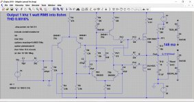
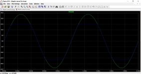
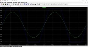
This shows 8 ohm and 4 ohm loading. The protection only triggers for the higher current 4 ohm load (blue trace).
This shows voltage across and current in a 4 and 8 ohm load with the protection circuit added.
In fact in simulation even those values seem to high. You would have to measure the real device and choose an appropriate rating to keep within the safe operating area for the FET.
This shows 8 ohm and 4 ohm loading. The protection only triggers for the higher current 4 ohm load (blue trace).
This shows voltage across and current in a 4 and 8 ohm load with the protection circuit added.
Attachments
It is very complicated to design effective short circuit or SOA protection. Given that the amps have been used for years without a problem I think the OP is better off being the protection himself by being careful not to short his speaker leads.
The gate source zeners, that are already internal to the FETs, are intended for anti-static protection during handling. They will prevent gate damage should the driver circuit go bananas. But they won't save the FET from being cremated during a prolonged short circuit condition.
I don't see how a simple zener clamp will both protect against a short circuit and allow adequate current peaks during normal operation.
Last edited:
Download the Lateral mosFET datasheet.So How easy is it to add a zener Gate Clamp to help protect against a short on the output, what voltage zener, it's current rating etc, the same goes for a zener across the Bias pot, what would we be looking at here.
What you need to understand is, I'm no designer, Yet I can repair a an aircraft flight computer, Head up display, etc with no problems, but the circuits have already been designed, I Know what signals are going in and I know what I should be seeing at the other end, so its not too difficult to work through the circuit to work out where things are going wrong, and I have been doing this for the last 30 years and up until recently where illness forced me to leave work.
Before that, I worked for a company that built Amstrad and Fidelity audio units (yeah, I know), I also had a period where I worked for myself repairing PA Equipment for local and not so local bands, Hundreds of blown 2N3055's, lots of Marshall amps where the Tubes glowed so brightly they lit up the room, due to the X Class Cap which supplied the -42 Bias voltage going O/C, and also TV and Video - (Shows how long ago that was) !!
But, give me a formula, and it might as well be written in Chinese, the same goes for Code, Macros etc, it's one of those things I can stare at for hours, and try to understand, but it just doesn't register.
So as people start to suggest adding zeners to help protect high gate voltages, that's fine, but do they simply connect between ground and the gate, or would there be additional circuitry involved, and as mentioned what voltages would we be looking at?
I hope that some you can understand my dilemma.
Find the SOA curves.
Look at the DC curve and find your supply rail voltage. Let's say that is 50Vdc
Now go up that voltage till you hit the DC SOA curve. It will cross at about 2A to 2.5A for all the single die 100W to 120W devices.
Now go up to the 100ms one shot line. It will probably be double, roughly 4A to 5A.
Now go higher to the 10ms or 1ms curve and note the allowed one shot current for which the device is safe.
It might be somewhere between 5Apk and 8Apk
Use that one shot transient "safe" current as a guide to the next stage.
Find the Vds vs Id plots. It has Vgs superimposed on it.
Go to the rail voltage as your Vds and go up to the power limit line. You now have the DC current where it crosses the Vds.
Let's continue with that last example where Vds=Vsupply = 50V
The 50Vds line cuts the 100W power limit at 2A for Id and the Vgs is shown as 3Vgs.
Now continue going up till you reach an Id equal to that transient value of ~7Apk. You are way above the DC ratings, but try to imagine where the Vgs plots are aiming.
The 7Vgs looks like it is aiming to asymtotically hit or very slightly exceed the 6A Id
This tells you that at 7Vgs and 50Vds, the maximum current the latFET will safely pass is ~6Apk, for a very short transient.
Select a Zener about that value to limit the transient current of the latFET to ~6Apk.
About 6v8, or 7v5 would do.
This is not the correct way to determine the Zener value but it gets the amp into the right ballpark.
There is a disadvantage in selecting the Zener as low as this. It limits the transient current when the speaker demands it.
A 1pair stage would do 6Apk
A 2pair stage would do 12Apk
A 3pair stage would do 18Apk
If your speakers demand very high transient currents you have to select the Zener to allow those peaks to pass (maybe a 9v1 Zener).
Connect the Zener from Gate to Source (it limits the gate to source voltage, Vgs).
The Zener will pass a high current if the driver or VAS sends that signal. The Zener will blow up the VAS if it triggers. You must fit a current limiting resistor between the VAS and Zener. The gate stopper can do this duty.
And use the Z+D as described by Mooly (post104).
And a final warning.
I used to think this would protect the amplifier from a shorted output.
But I was corrected some years ago.
A very fast Current change (like an inadvertant spkr cable short) takes the FET outside it's safe operating envelope (V/us or I/us) and will fail.
That particular discussion was in a vertical mosFET Thread, the latFET may be more tolerant of this failure mode.
Last edited:
It also depends on how capacitive the speaker load is.
Into a pure 8-ohm resistor, peak, instantaneous FET power occurs when Vds = Vout. For 50V rails it's about 80W. For 40V rails it is about 50W. The average power per FET is much lower.
If the circuit tried to drive a pure capacitor max sinewave current would occur when Vds=50V and if the cap was large enough the FETs would be toast.
Last edited:
Thank you all for your replys.
So Really the zener is only to protect against an accidental short on the output, I have always had a method when connecting and amp to the speakers.
1. Don't connect while the amp is on.
2. Make sure the cables have a little slack, should the amp be moved.
3. Ensure the binding posts are tight, and the cables can't be pulled out.
4. Check (now my eyes are not so great) with a x10 eyeglass that no whiskers or strands have come astray and could short to the other terminal.
Without a fast reacting DC detection circuit in place, I don't really see that the speakers could be protected should one of the output devices fail, my only hope is that the fuses might blow in time.
The Zener across the Bias Pot is a good idea should a problem occur with the pot itself, and I still have the original open track type fitted, which does worry me a little, but I do intend to replace these, 470R and 500R have been suggested, 470R would probably be easier to get hold of in the original encapsulated and pin spacing style, A 500R would probably need to be of the 10 - 25 turn cermet style, I'm not really too bothered the cermet would almost certainly give a little more control.
Traderbam, Thank you for the link to the alternative caps, While I have been looking at different caps for this part of the circuit, and ones where I don't have to buy 25 at 50p each, or ones that cost £8.00+ Each, I had been looking for a smallish cap with leads long enough to reach where they need to go, but at the same time wondering, would a small cap with long leads negate what we are trying to achieve here, so did actually wonder if a big cap with a pin spacing large enough to reach across the tracks but with short leads be better, the pin spacing would need to be about 30 - 35mm.
The Gate resistors, I intend to fit zero ohm links where the original resistors are fitted, and cut the tracks near the gate pins and fit SMD Resistors.
Thanks again for all of the posts and suggestions.
The Hitachi/Maplin design avoids the VAS current problem by limiting current to about 13mA. This allows the zener to be connected to the VAS end of the gate stopper and avoids the RF stability issues of long tracks on the gate.Connect the Zener from Gate to Source (it limits the gate to source voltage, Vgs). The Zener will pass a high current if the driver or VAS sends that signal. The Zener will blow up the VAS if it triggers. You must fit a current limiting resistor between the VAS and Zener. The gate stopper can do this duty.
And use the Z+D as described by Mooly (post104).
And a final warning.
I used to think this would protect the amplifier from a shorted output. But I was corrected some years ago. A very fast Current change (like an inadvertant spkr cable short) takes the FET outside it's safe operating envelope (V/us or I/us) and will fail. That particular discussion was in a vertical mosFET Thread, the latFET may be more tolerant of this failure mode.
The output inductors second purpose is to prevent these fast transients getting to the FET.
Speaker fuses are always an option and can be incorporated within the feedback loop. Sized correctly they offer great protection.
Bias pots are something I always anticipate replacing with fixed resistors. When making PCB allow for a couple of series/parallel parts to be fitted to get the correct value that a temporary pot was set to. Once initially set there is no reason for bias to alter and require resetting at a later date.
Bias pots are something I always anticipate replacing with fixed resistors. When making PCB allow for a couple of series/parallel parts to be fitted to get the correct value that a temporary pot was set to. Once initially set there is no reason for bias to alter and require resetting at a later date.
There is no advantage here to use the larger sized caps. I would choose the smaller ones myself as I would find them easier to fit. You need 4 and they come in packs of 5.Traderbam, Thank you for the link to the alternative caps, While I have been looking at different caps for this part of the circuit, and ones where I don't have to buy 25 at 50p each, or ones that cost £8.00+ Each, I had been looking for a smallish cap with leads long enough to reach where they need to go, but at the same time wondering, would a small cap with long leads negate what we are trying to achieve here, so did actually wonder if a big cap with a pin spacing large enough to reach across the tracks but with short leads be better, the pin spacing would need to be about 30 - 35mm.
There is no advantage here to use the larger sized caps. I would choose the smaller ones myself as I would find them easier to fit. You need 4 and they come in packs of 5.
Ok, Thanks for clearing that up, I'll get some on order
Bias pots are something I always anticipate replacing with fixed resistors. When making PCB allow for a couple of series/parallel parts to be fitted to get the correct value that a temporary pot was set to. Once initially set there is no reason for bias to alter and require resetting at a later date.
I agree, and did think that that would be better, A decade box would come in handy, unfortunately, I no longer have access to one
More envelope jottings. In theory, driving a pure capacitor of 1uF at 20kHz sinewave and 50V peak would draw a peak current of about 6A when Vout=0V. Let's say the psu is 50V, then that's 300W instantaneous FET power; nearly 4 times that for an 8 ohm resistor. Assuming the amp is stable.
Of course, speakers aren't usually 1uF capacitors at 20kHz and the amp has an output inductor.
Of course, speakers aren't usually 1uF capacitors at 20kHz and the amp has an output inductor.
![2017-09-25 20_34_05-[ MaplinV2 _].png](/community/data/attachments/578/578974-73b2895bf92ae99e993e29f93a9edfd1.jpg)
One thing I forgot to mention in my earlier post, and really goes back to how this thread started, was the temp of the output transistors.
At Idle they will settle at about 30°C, But feeding a 7.5 ohm Dummy Load with a 25v pk-pk 1khz sine wave they soon reach around 61°C
To me that seems excessively hot, and doing the calculations only equals about 10.4 watts
I have modified the way the amps are mounted to the heatsinks from the original way I had them, but it doesn't seem to have made much difference.
What else also bothers me, is the fact that the temperature difference between the transistor cases and the and the mounting bracket they are bolted to is 10°C lower, I haven't used SIL Pads, not a fan of them, but Mica Washers and thermal paste, Like the good old Dow Corning stuff, and applied it with a small brush to get a nice even coating.
Ideally the transistor temperature and whatever its bolted to should be a close as possible, although probably not totally achievable, but 10°C does seem a bit excessive to me, would appreciate anyone else's Thoughts / Experience on this.
More envelope jottings. In theory, driving a pure capacitor of 1uF at 20kHz sinewave and 50V peak would draw a peak current of about 6A when Vout=0V. Let's say the psu is 50V, then that's 300W instantaneous FET power; nearly 4 times that for an 8 ohm resistor. Assuming the amp is stable.
Of course, speakers aren't usually 1uF capacitors at 20kHz and the amp has an output inductor.
I dare say Mrs DiyGazza would be happy if I got rid of my speakers and replaced them with a pair of caps that could be hidden away
http://www.ti.com/lit/an/sboa020/sboa020.pdf
See Table II
Eg: if the thermal resistance between FET and bracket is 0.4C/W and you are seeing a 10C temperature difference, the FET must be dissipating about 25W (neglecting heat loss to air and PCB traces).
The RMS current in the resistor is 12.5/7.5/1.4 = 1.2A.
During each half cycle each FET might dissipate somewhere between (50-12.5)*1.2=45W and 50*1.2=60W, or between 23W and 30W average over a full cycle.
In the right ballpark.
Edit: Using a spreadsheet gives 21.2W. Still not far off your bench measurements and the thermal resistance is a guess. This is the price for having high power rails - poor efficiency at low power outputs.
Last edited:
http://www.ti.com/lit/an/sboa020/sboa020.pdf
See Table II
Eg: if the thermal resistance between FET and bracket is 0.4C/W and you are seeing a 10C temperature difference, the FET must be dissipating about 25W (neglecting heat loss to air and PCB traces).
The RMS current in the resistor is 12.5/7.5/1.4 = 1.2A.
During each half cycle each FET will dissipate somewhere between (50-12.5)*1.2=45W and 50*1.2=60W, or between 23W and 30W average over a full cycle.
In the right ballpark.
Aha, Thank you for working / (Explaining) that out. As I mentioned, a formula I can stare at for ages, and it makes no sense, But give the formula with an example, then I can start to make sense of them.
So looks like we're good
- Status
- This old topic is closed. If you want to reopen this topic, contact a moderator using the "Report Post" button.
- Home
- Amplifiers
- Solid State
- Any Maplin MosFet Amp Guru's on here?