Yes... Seems so...
Btw following your threads on Nos Filters (which went in the direction of recording quality) and the tda1543 ozone over at WBF.
What is your take on tda1387? I actually believed thia may be the mysterious uda1305at used in the amr cd777. At least its multibit, compared to cc of the tda1305...
Btw following your threads on Nos Filters (which went in the direction of recording quality) and the tda1543 ozone over at WBF.
What is your take on tda1387? I actually believed thia may be the mysterious uda1305at used in the amr cd777. At least its multibit, compared to cc of the tda1305...
I like the TDA1387 but it takes about double the power of the TDA1545A so I'll use this one when I need lowest power. I'm using TDA1387 on Ozone because power isn't an issue and its I2S just like TDA1543 so no mods are needed to the digital stuff. I rather suspect that the cd777 uses TDA1545A because its a bit more flexible in programming the bias current and I know Thorsten likes to run it a bit hotter than normal 
No, its highly unlikely to be 1543, I seem to recall the measurements looked too good for that. Also when the output stage is valve, the designer can afford more glitches because a valve has better HF linearity, hence no major drawback to using CMOS over bipolar I'd have thought. So it would be an extremely odd choice if it were the 1543.
For those of you that are into TDA1541. This unit Nakamichi DAC101 intended for car audio has an interesting dual TDA1541 S1 single crown in differential mode. They show up on Ebay from time to time. I bought one for $100,- and who knows what a little tweaking and modification can reveal.
Attachments
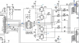
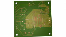
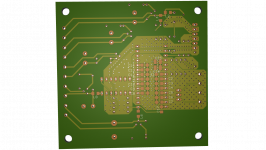
My layout
Here is the layout I am working on. It is simpler than the full reclocker that has been suggested. I have a layout with the full reclocker, but am not really happy with it, also, with the reclocker circuits others are working on, I'm not sure it is necessary. Also, the source I would be using for the time being is usb using a 12mhz clock. So this is a simple one incorporating some of the recommendations from this thread. What do you guys think. Any changes that should be made, or is it worth a try.
Thanks
Chris
Attachments
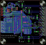
Cmon boys, the layout is rather weird for me - bypasses are weird (i prefer using ground plane as is, and throw the bypass cap as close as possible. To feed the PS trace first thru cap, and then by wide (same width as cap's footprint) trace into IC's pin.
Then the I2S thing... Why those bulky thruholes? Digital is all-SMT world. I still regret i haven't used 0804 in my PCB /but i have my reasons - i've got loads of 1206 in E96 series values. I'll settle on some specific resistor values for 3.3 / 5v logic levels and then go 0804/.
HC02... same thing, why DIP? And if you use just a tiny part of it, why not go with single/dual gates? they are nicier, less substrate bounce as their package is tinier.
Oh, what's characteristic impedance of your digital traces, do they match the characteristic impedance of your source and u.fl connectors/coax?
Do your digital traces have ground cuts underneath the traces?
I've said 13 times "it's release" prior to sending the PCBs to production - and i still got some minor mistakes
Just take some nice book on digital design, like "black magic" of HJ, plus some EMC docs ( EMC Information Centre - The EMC Journal (Free in the UK) is a good place to start, as well as many appnotes on EMC and digital/mixed signal PCB design).
Watch out the current flow. It flows thru trace and always returns back to the place where it came from - it's The Loop, which area you want to keep as small as possible.
Return currents of traces flow under the trace, in the ground plane. If you cut the plane under the trace, the current will have to find other ways around to get back - and they don't care of flowing thru the air, making-up some nasty EMI emissions.
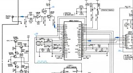
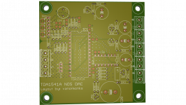
Latest
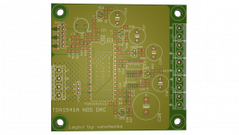
Thanks for the advice. I have made some changes. The through hole was mainly because I am more comfortable with it, and the tda1541a is through hole also. But here we go.
As far as the impedance of the traces, I don't know how to determine that, and don't have the equipment even if I did. But My goal is not really the best ever created. In fact, I was planning on purchasing your board when finished, although last I checked it seamed you were going for a slaved source setup. Mainly I wanted to try a basic universal tda1541a Dac, that is simple to construct and incorporates many of the elements that have been found to improve the sound. And I have never done a digital layout before, and nothing seems available that meet what I'm looking for.
Which is why I appreciate the help, and hopefully the following looks better.
Also, could you explain what you mean by ground cuts underneath the traces.
Thanks,
Chris
Cmon boys, the layout is rather weird for me - bypasses are weird (i prefer using ground plane as is, and throw the bypass cap as close as possible. To feed the PS trace first thru cap, and then by wide (same width as cap's footprint) trace into IC's pin.
Then the I2S thing... Why those bulky thruholes? Digital is all-SMT world. I still regret i haven't used 0804 in my PCB /but i have my reasons - i've got loads of 1206 in E96 series values. I'll settle on some specific resistor values for 3.3 / 5v logic levels and then go 0804/.
HC02... same thing, why DIP? And if you use just a tiny part of it, why not go with single/dual gates? they are nicier, less substrate bounce as their package is tinier.
Oh, what's characteristic impedance of your digital traces, do they match the characteristic impedance of your source and u.fl connectors/coax?
Do your digital traces have ground cuts underneath the traces?
I've said 13 times "it's release" prior to sending the PCBs to production - and i still got some minor mistakes
Just take some nice book on digital design, like "black magic" of HJ, plus some EMC docs ( EMC Information Centre - The EMC Journal (Free in the UK) is a good place to start, as well as many appnotes on EMC and digital/mixed signal PCB design).
Watch out the current flow. It flows thru trace and always returns back to the place where it came from - it's The Loop, which area you want to keep as small as possible.
Return currents of traces flow under the trace, in the ground plane. If you cut the plane under the trace, the current will have to find other ways around to get back - and they don't care of flowing thru the air, making-up some nasty EMI emissions.
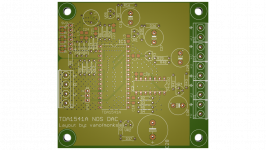
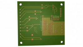
Thanks for the advice. I have made some changes. The through hole was mainly because I am more comfortable with it, and the tda1541a is through hole also. But here we go.
As far as the impedance of the traces, I don't know how to determine that, and don't have the equipment even if I did. But My goal is not really the best ever created. In fact, I was planning on purchasing your board when finished, although last I checked it seamed you were going for a slaved source setup. Mainly I wanted to try a basic universal tda1541a Dac, that is simple to construct and incorporates many of the elements that have been found to improve the sound. And I have never done a digital layout before, and nothing seems available that meet what I'm looking for.
Which is why I appreciate the help, and hopefully the following looks better.
Also, could you explain what you mean by ground cuts underneath the traces.
Thanks,
Chris
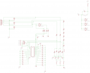
Attachments
Last edited:
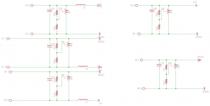
TDA sounds best with shunt regulators near the pins (TL431). It is so important to good sound with this chip, that there is no point to making a board without it IMO.
Also, I would suggest the thickest possible traces for the LR current output pins.
Is the TL431 really a good choice? If you went smt with potado logic and dropped the TL431's you could have a really small board that could butt right next to salas regs.
As far as the tda cap decoupling yours is the best board I've seen. I don't see and cuts in the ground plan except the ground connects to the caps they aren't the correct ones to use you want pads that have continous contact to the ground plane they are smd caps but you have odd connection to ground, they look like thru hole.
Yours is a slaved source setup too. I think you have outdone all other recent attempts. As far as the trace impedance there are formulas for calculating also terminating the ufl connector with a resistor is important. I bet you can make this simple board the best out there with just a little more research. You can probably find it on a search. I think something like this would be very useful for a lot of us.
There isn't much else out there besides the terrible raindrp china boards and the rb boards have many mistakes.
Thanks for sharing.
no, with solid ground planes and small SMD, using spoked SMD ground pads is perfectly reasonable, you will find Ian uses these often too, it makes the board much more solderable and at these currents really doesnt have any disadvantage.
to terminate or not... hmm depends, the transport/TX is terminated already and if the connectors are consistent with the impedance, I dont think its so cut and dried that you must terminate every u.fl at both ends
to terminate or not... hmm depends, the transport/TX is terminated already and if the connectors are consistent with the impedance, I dont think its so cut and dried that you must terminate every u.fl at both ends
Last edited:
- Status
- This old topic is closed. If you want to reopen this topic, contact a moderator using the "Report Post" button.
- Home
- Source & Line
- Digital Line Level
- Any good TDA1541A DAC kit?