
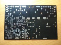
I'll echo Choco's comments; thank you for sharing an interesting build and Kemp's MSE thesis. Do you have measurements of your build? The structure of Kemp's THD+N results is promising and I'll have to get your self-oscillating variant into sim for a closer look.
1) Any particular reason for selecting the LM319 over, say, a TL3016?
2) Is the value of R97 correct? <1Hz is an interestingly low cutoff to Vdd.
A minor comment: both this and the other schematic may be missing a lowpass cap on the + input of the DA1.2 difference amplifier. C37 requires a peer to maintain CMRR both above and some octaves below the lowpass corner frequency.
Also, most results I've seen show some improvement with larger values of C73 than used here. That, along with increasing C74, may be something to try. I like the supply symmetry between Vcc and Vb but wonder if a better result might be obtained without the two ohm resistors and diodes of lower dynamic impedance than 1N4148s.
The LM317 and LM337 for the MOD supplies should probably have protection diodes to discharge +-12V when the supply is turned off. Most datasheets besides National's and TI's 317s are hazy as to when they are required, though.
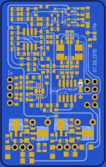
Cool! Two immediate questions:Diagram
1) Any particular reason for selecting the LM319 over, say, a TL3016?
2) Is the value of R97 correct? <1Hz is an interestingly low cutoff to Vdd.
A minor comment: both this and the other schematic may be missing a lowpass cap on the + input of the DA1.2 difference amplifier. C37 requires a peer to maintain CMRR both above and some octaves below the lowpass corner frequency.
Also, most results I've seen show some improvement with larger values of C73 than used here. That, along with increasing C74, may be something to try. I like the supply symmetry between Vcc and Vb but wonder if a better result might be obtained without the two ohm resistors and diodes of lower dynamic impedance than 1N4148s.
The LM317 and LM337 for the MOD supplies should probably have protection diodes to discharge +-12V when the supply is turned off. Most datasheets besides National's and TI's 317s are hazy as to when they are required, though.
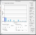
Thank you for the info. I wonder how much of that THD is measurement floor.
Interesting twist to take out the Vb diode and just let the long RC time constant stabilize the supply. I'll have to give that a closer look.
On the regulators National and TI both indicate protection diodes above 250uC or so. This build's above that by an order of magnitude. More likely to be a long term reliability issue than an immediate failure.
Interesting twist to take out the Vb diode and just let the long RC time constant stabilize the supply.
The IRS20957 has this protective Z-diode integrated, it is needed in situations when the start up resistor R104 delivers more current than the high side driver needs.
Yah, I haven't checked every datasheet but probably all of IRF's audio half bridge drivers have Vb and Vcc zener clamps. There is some variation between 15 and 20V clamping from part to part but the application schematics consistently show an external Vb diode.
What I was referring to by RC stabilizing the supply is without the Vb diode there's current through the supply resistor back to Vcc when the high side FET is on. I'd need to look at sim to say if there's an efficiency penalty, though since the supply resistor here is lower impedance than most diodes it's probably not significant if it's not a win. Also a little more thinking about high side supply UVLO is required.
What I was referring to by RC stabilizing the supply is without the Vb diode there's current through the supply resistor back to Vcc when the high side FET is on. I'd need to look at sim to say if there's an efficiency penalty, though since the supply resistor here is lower impedance than most diodes it's probably not significant if it's not a win. Also a little more thinking about high side supply UVLO is required.
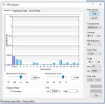

is this approaching ncore performance levels?
...if it was measured at 1W, then it is LiteAmp level.
If it was measured at half power then it is ncore level.
- Status
- This old topic is closed. If you want to reopen this topic, contact a moderator using the "Report Post" button.
- Home
- Amplifiers
- Class D
- Amp