Hi Guys,
Please use the updated schematic I've attached. I forgot the 221 ohm gate resistors, and they should be added. The rest of the schematic is the same, and it's correct. Sorry for the omission.
Cheers,
Owen
ChuckT: Try 600 ohms and 1300 ohms for about 1 VRMS output. At that resistance you're probably fine to omit the B1 buffer section, but you might want to make sure you're not driving too low an input impedance on the next stage. When those upper two resistors start creeping over 1k, I'd suggest putting the buffer back in.
Attachments
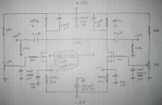
The trimpots are used to adjust the gate voltage, and hence the voltage present at the source of the mosfet (above the 400 ohm resistors).
Before startup, I would disconnect from the DAC, and set both trimpots to minimum (0 ohms). Increase the value of the trimpots to set the voltage at the source of each of the two fets to 1.65VDC referenced to ground. Once this is done, verify that the voltage at the drain is about 9VDC referenced to ground. If all is good, power down, connect to the DAC output, and start back up. You may need to re-adjust to get exactly 1.65V at each source, but it shouldn't have changed much.
The value of the pot will vary from mosfet to mosfet, so there is no set value for it. If you are using matched fets, you'll get about the same value for each one, but there's no way to tell what value will get you what you need for voltage. Once this is adjusted, I would let the unit run for a few days, then re-check and re-adjust, and you'll be good to go.
If this still seems confusing, let me know and I can draw up a diagram.
Cheers,
Owen
Hi Owen,
I was looking at the circuit and it occurs to me that the time constant for the gate voltage is much longer than the supplies coming up. Therefore, I would suspect that upon power up the voltage at the source of the MOSFETs would start off negative (because the gate starts at ground) and then slowly rise up to the steady state value as the gate capacitor is charged up.
I am using the PCM1794; and I fear that during power on the current output pins of the DAC chip will be "pulled" negative for a short time. The datasheet specifies a maximum of 10mA current on any pin. I plan to run a simulation of this, but I do not have a model for the DAC output.
Preliminary calculations say that if the DAC chip has an internal diode to ground (for ESD protection) the current will exceed MAX ratings. esentially you have a 400 ohm resistor to -18V for some time until the MOSFET turns on and stabilizes.
Just thought I would mention this to you and see if you thought about it any. I don't see an "easy" solution and I will most likely try the circuit anyway. Hopefully the DAC chip can handle this transient without damage; unfortunately, it can last a long time depending on the time constant used to filter the DC bias on the gates.
Hi Owen,
thanks for posting this interesting i/v schematic,
i would like to know two things:
1) can the i/v circuit on post #61 be used without change both with buffalo24 (es9008) and buffalo32 (es9018)?
2) can i omit the 10uF out capcitors if i use a transformer to have an unbalanced out?
Thanks
Ciao
Andrea
how this compare to original D1 i / v
ChuckT are you using your i / v with pcm63
Nope, I use pcm1702, similar but lower current output.
I haven't try Owen circuit yet, but I have try one diff mosfet (K216) on the D1 and it sound fairly similar to the irf610.
Hi Guys,
Lots of questions... I'll try to address each in order:
ChuckT: 1300 ohms would replace the 400 ohms, and 600 ohms would replace the 185 ohms. This should give you about 1VRMS if you use it in the circuit posted. If you use +/-30V supplies then dissipation might be a little on the high side, and I'm not sure how well it will work. If you want something drastically different then I'd suggest trying LTspice to simulate it first. It's free, and I could even send you the schematic files to try.
samoloko: I had a D1 output stage replacing the op-amp stages in my Resolution Audio CD-50 for a long time, and it was driven by 4 PCM63's just like in the original D1. I liked this setup, but I much prefer the new buffalo DAC with this I/V stage. It's too hand to directly compare both since the DAC's are so different. Today's DAC's output WAY more current than the last generation, which makes the circuit I'm using possible.
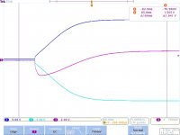
Jmertz: Very valid concern, and excellent question. I pulled out the scope, and measured the transient at the input during startup. I've attached the screenshot from the scope, which was taken under normal startup with no DAC attached. The input node swings negative to about -2.9V (this is worst case, I tried it about 20 times on different inputs) before it climbs steadily up to 1.65V. I'll have to consult the datasheet for the DAC, but it should be fine. I might try again today with the DAC attached just to see how that looks.
anbello: Yes, this circuit can be used exactly as it is with either of those DACs. As for the transformer, you could probably omit both caps if you take the time to balance to voltage to an equal value at each drain. Once that's done, you can attach the transformer and you should be good to go. Otherwise, you can use just one capacitor on either side, or between the two primaries if your transformer is setup like that. Either way, you don't need two caps.
Cheers,
Owen
Lots of questions... I'll try to address each in order:
ChuckT: 1300 ohms would replace the 400 ohms, and 600 ohms would replace the 185 ohms. This should give you about 1VRMS if you use it in the circuit posted. If you use +/-30V supplies then dissipation might be a little on the high side, and I'm not sure how well it will work. If you want something drastically different then I'd suggest trying LTspice to simulate it first. It's free, and I could even send you the schematic files to try.
samoloko: I had a D1 output stage replacing the op-amp stages in my Resolution Audio CD-50 for a long time, and it was driven by 4 PCM63's just like in the original D1. I liked this setup, but I much prefer the new buffalo DAC with this I/V stage. It's too hand to directly compare both since the DAC's are so different. Today's DAC's output WAY more current than the last generation, which makes the circuit I'm using possible.
Jmertz: Very valid concern, and excellent question. I pulled out the scope, and measured the transient at the input during startup. I've attached the screenshot from the scope, which was taken under normal startup with no DAC attached. The input node swings negative to about -2.9V (this is worst case, I tried it about 20 times on different inputs) before it climbs steadily up to 1.65V. I'll have to consult the datasheet for the DAC, but it should be fine. I might try again today with the DAC attached just to see how that looks.
anbello: Yes, this circuit can be used exactly as it is with either of those DACs. As for the transformer, you could probably omit both caps if you take the time to balance to voltage to an equal value at each drain. Once that's done, you can attach the transformer and you should be good to go. Otherwise, you can use just one capacitor on either side, or between the two primaries if your transformer is setup like that. Either way, you don't need two caps.
Cheers,
Owen
Attachments
Thanks Owen,
If you get around to powering it up with the DAC chip connected please post the scope shot. Thanks!
Unfortunately the data sheet for the PCM1794 is not very detailed. I think the only way I will know is to try it.
I wonder if anyone else has used the D1 I/V with the PCM1794?
If you get around to powering it up with the DAC chip connected please post the scope shot. Thanks!
Unfortunately the data sheet for the PCM1794 is not very detailed. I think the only way I will know is to try it.
I wonder if anyone else has used the D1 I/V with the PCM1794?
Hi Guys,
Please use the updated schematic I've attached. I forgot the 221 ohm gate resistors, and they should be added. The rest of the schematic is the same, and it's correct. Sorry for the omission.
Cheers,
Owen
ChuckT: Try 600 ohms and 1300 ohms for about 1 VRMS output. At that resistance you're probably fine to omit the B1 buffer section, but you might want to make sure you're not driving too low an input impedance on the next stage. When those upper two resistors start creeping over 1k, I'd suggest putting the buffer back in.
Good work Owen, you have really stripped it down to the essentials.
")
It looks like the phase is reversed on the outputs. Output phase will be the same as the input phase on each side.
I have used common gate FET stages just like this, and they do indeed sound great.
Cheers!
Russ
Russ, I think the phase depends on the DAC chip used.
I am looking to use this stage with the PCM1794 and in this case the polarity is reversed from that of the DAC chip pinout.
The PCM1794 chip datasheet assumes the use of an op-amp I/V stage. In which case a positive going output current will result in a negative going voltage. However, with the common gate stage a positive going input current results in a positive going output voltage.
So in the case of the PCM1794; the +IN will become the -OUT.
This was confusing to me, but it makes sense that they labeled the outputs from the chip assuming that most people will use an opamp I/V as recommended.
Hi, In regard to this stage the phase is what it is. It won't matter what DAC is used.
At the input of one side of the this particular I/V stage the output is the same phase on the same side. It is essentially two single ended non-inverting circuits.
I was just pointing that out because the schematic shows the it is the opposite phase, which is not correct. Though its certainly not a big deal for a balanced stage.
Cheers!
Russ
It won't matter what DAC is used. At the input of one side of the this particular I/V stage the output is the same phase on the same side. It is essentially two single ended non-inverting circuits.
I was just pointing that out because the schematic shows the it is the opposite phase, which is not correct. Though its certainly not a big deal for a balanced stage.
Cheers!
Russ
Russ, I think the phase depends on the DAC chip used.
The PCM1794 chip datasheet assumes the use of an op-amp I/V stage. In which case a positive going output current will result in a negative going voltage. However, with the common gate stage a positive going input current results in a positive going output voltage.
So in the case of the PCM1794; the +IN will become the -OUT.
I understand what you are saying. Some parts (like PCM1794A) are labeled with the polarity of the current, but in reality at the input of the I/V stage (even an opamp I/V) it still is a very real voltage. Notice that this still holds true even in the TI datasheet.
You will notice that despite the labels attached to the DAC outputs, the opamp symbols on the DS example are still correct regarding the voltage.
In any case I was only mentioning it in passing, in practice its not very important. But in the case of the ESS DAC the output is very correctly modeled as a voltage with an impedance of 195 ohms. So at least with regard to those chips, it is wise to understand that there is a voltage behind the current.
In any case, I did not want to come off critical. Its ok if he meant IN- to mean inverse current, but that will mean using the non-inverse output to get inverse current from the ESS chip.
Cheers,
Russ
Last edited:
fair enough.
It was just something I noticed when I was making a prototype with the PCM1794. I am only using one of the outputs since I just have a single-ended I/V stage. When I looked at the datasheet it occured to me that in order to get the "correct" polarity of the audio signal (not inverted), I had to use the signal coming from the minus output pin of the DAC chip into my I/V stage.
However, if I use an opamp I/V instead of the C-Gate stage. I would then use the positive current output pin.
Just wanted to let Owen and others know, in case he did not realize this.
Does this make sense? I am pretty sure this is correct, but it is always good to have another set of eyes.
Here's my logic:
opamp I/V--> increasing input current (going into the input node) causes the output voltage to decrease
C-gate stage--> increasing input current causes the output voltage to increase.
So even though they both convert current into voltage; the opamp stage has an inverted voltage signal compared to the C-gate stage.
To get the same polarity out of the DAC chip, you have to select the proper output pin depending on the I/V stage used.
Please check me on this.
- Status
- This old topic is closed. If you want to reopen this topic, contact a moderator using the "Report Post" button.
- Home
- Source & Line
- Digital Line Level
- A New Take on the Classic Pass Labs D1 with an ESS Dac