Hi all,
I have read a lot of threads here and I have a simple question regarding class D amps you can with out a doubt answer me")
One of the more expensive parts in an amplifier is the transformer it adds a lot of weight and is expensive.
Has anyone done a class D amp with one 320V rail ?
Just the 230V and a rectifier, no trans.
I know it could simply kill anyone who is trying to connect the speakers while the amp is on, but this is DIY, I'm willing to bet a few bucks that you don't let people mess around with your equipment
The output stage would be a mosfet, and a small transformer, somewhat like the valve amplifiers use. (Why not do PWM at 1MHZ?)
The "front" side of the transformer would be from the +320V to ground through some high frq mosfet.
The "back" side of the trans would some feedback circuit and a lpf to the speaker.
Would this be at all doable or are the some major flaws in doing an amp like this ?
Best regards,
Gunnar I. T.
I have read a lot of threads here and I have a simple question regarding class D amps you can with out a doubt answer me
One of the more expensive parts in an amplifier is the transformer it adds a lot of weight and is expensive.
Has anyone done a class D amp with one 320V rail ?
Just the 230V and a rectifier, no trans.
I know it could simply kill anyone who is trying to connect the speakers while the amp is on, but this is DIY, I'm willing to bet a few bucks that you don't let people mess around with your equipment
The output stage would be a mosfet, and a small transformer, somewhat like the valve amplifiers use. (Why not do PWM at 1MHZ?)
The "front" side of the transformer would be from the +320V to ground through some high frq mosfet.
The "back" side of the trans would some feedback circuit and a lpf to the speaker.
Would this be at all doable or are the some major flaws in doing an amp like this ?
Best regards,
Gunnar I. T.
Hi Lars,
Do you have schematics for the amplifier you would be willing to share with the rest of us ?
Why do you think most class d amps use +- 70/50/30/24 rails ?
Is it easier to build? less hazardus (sp?) ? cheaper components ?
Is it hard to get the output trans ?
All the best from Iceland,
Gunnar.
Do you have schematics for the amplifier you would be willing to share with the rest of us ?
Why do you think most class d amps use +- 70/50/30/24 rails ?
Is it easier to build? less hazardus (sp?) ? cheaper components ?
Is it hard to get the output trans ?
All the best from Iceland,
Gunnar.
Gunnar: When you go above 200V (rail to rail) the MOSFET's tend
to get a much higher on-resistance, resulting in poorer efficiency of the
amplifier. Component price is more or less the same.
For audio i would probably rather have a slow and unlinear componnet as the transformer in the power supply, than in series with the output. That might be the reason you are looking for ..
GunnarIT said:LOL
Lars, thank you for good answers.
And if anyone comes across any links or schematics of transformerless Class D amps then please post it on this thread
Best regards,
Gunnar I. T.
Here you are:
http://www.flyingmole.co.jp/en/index.shtml
Everythin integrated on one circuit board and no transformer.
This stuff seems to be quite popular in Japan
Best regards
Gertjan
Not the answer that you were looking for........
But if you have enough $$$$$, in theory, you could buy one of these:
http://www.diyaudio.com/forums/showthread.php?postid=403502#post403502
Jocko
But if you have enough $$$$$, in theory, you could buy one of these:
http://www.diyaudio.com/forums/showthread.php?postid=403502#post403502
Jocko
I once saw a proposal in a book (by Ben Duncan ??) that was called ampliverter. This was basically an SMPS capable of positive and negative putput voltages, by using some sort of selectable rectifier on the secondary of the transformer. That way it was possible to use an SMPS transformer of the usually small size.
Keep in mind that if you had to transform the output signal right after an ordinary class-d amp (running at a high voltage) you'd have to use an ordinary sized audio transformer.
Another topology is used by Peavey. They use two SMPS that are running a the same frequency, both at a constant duty-cycle of 50%. One of the "carriers" is modulated in phase, proportionally to the input voltage, and the secondaries of the transformers are summed by synchronous rectification. After the rectification you have a PWM signal which can then be low-pass filtered in the usual way.
http://l2.espacenet.com/espacenet/viewer?PN=US4992751&CY=ch&LG=de&DB=EPD
Regards
Charles
Looks that B&O has different opinion. Look at this patent application http://appft1.uspto.gov/netacgi/nph...p=1&u=/netahtml/PTO/srchnum.html&r=0&f=S&l=50.A transformerless amp would never be approved in Europe and and in 230 V country.
IMHO it would be posssible provided:
it is mounted in the loudspeaker cabinet
has optical input
non flammable speaker membrane and coil
protectively earthed non detachable metal speaker grill
Best regards,
Jaka Racman
Another topology is used by Peavey. They use two SMPS that are running a the same frequency, both at a constant duty-cycle of 50%. One of the "carriers" is modulated in phase, proportionally to the input voltage, and the secondaries of the transformers are summed by synchronous rectification. After the rectification you have a PWM signal which can then be low-pass filtered in the usual way.
Hi Charles,
your description is not entirely accurate. There is one primary oscillator runing at 50% duty cycle. Secondary is demodulated by bidirectional switches run at 50% duty cycle and phase shifted towards primary. I have extensively simulated topology in 1999 not knowing it has already been patented
 . It has some interesting properties like doubling of filter ripple frequency and zero voltage switching for some of the switches. The only difference with the patented circuit was that i used back to back (source and gate tied together) connected mosfets for bidirectional switches instead of mosfet inside diode bridge as Peavey uses.
Do you know if the patented circuit is actually used in a product?
Best regards,
Jaka Racman
I worked together with Brian Attwood for a couple of months during the research phase of a class d project some years ago. We had some interesting luch time discussions.Originally posted by Jaka Racman
Hi Charles, your description is not entirely accurate. There is one primary oscillator running at 50% duty cycle. Secondary is demodulated by bidirectional switches run at 50% duty cycle and phase shifted towards primary. I have extensively simulated topology in 1999 not knowing it has already been patented
Do you know if the patented circuit is actually used in a product?
He is a very pleasant man of high integrity (although a little bit of a lone wolf). I specifically asked him about that design one day because a friend of mine had done something very similar in order to make a sine wave dc to ac inverter (he used back to back mosfets for the bilateral switches). My friend could not come up with a simple, passive circuit to recycle the leakage energy dumped when the bilateral switches turned off and ended up using clamping diodes to a couple of caps that were then bled off back to the input by a separate little power converter. After much blood, sweat and tears, my friend got his prototype working reliably, but concluded that it was more expense and trouble than the traditional sine wave inverter approach using an intermediate high voltage dc link.
So, Jaka, how did your design deal with this problem?
By the way, Brian Attwood said that he thought that perhaps the main advantage of that class d amp topology was that a lot of the non idealities (offsets, delays, etc.) in the two phased carriers tended to cancel each other in the final output. (Never looked into it myself - what did you find?)
Regards -- analog(spiceman)
Jaka Racman said:
...
Do you know if the patented circuit is actually used in a product?
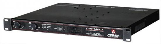
I guess it is this one: Peavey DPC1400X
Attachments
I toyed with the idea of a line operated class D over a year ago, for high power and to get ride of a high power PSU. Did not pursue it further for it turned out to be no great improvement in comparison with a conventional one.
The concept can be better understood thinking of it as a conventional switcher supply, only providing a variable output voltage instead of DC.
One approach should require a large DC blocking output capacitor, with the quiescent "supply" output at half maximum output corresponding to a 50% duty cycle driven totem-pole. Note this requires the power switches to be driven independently and balanced from 0 to 50% so as to ramp from 0 to full and at the same time avoiding net DC on the transformer.
A second approach should be dual paralell switching chains, one each for the positive and negative signal excursions. This requires additional controlled switches to short the inactive side to ground so as to provide a return path for the active side.
Not that I think unfeasible either way, but still see no huge benefit.
Comments welcome!!
Rodolfo
Hi,
at the end I decided that the leakage inductance of the transformer would be a major drawback and never got past the simulation stage. That's why I asked if there is a real circuit behind the patent.
Thanks for sharing a real life experience with the circuit.
Best regards,
Jaka Racman
at the end I decided that the leakage inductance of the transformer would be a major drawback and never got past the simulation stage. That's why I asked if there is a real circuit behind the patent.
Thanks for sharing a real life experience with the circuit.
Best regards,
Jaka Racman
More...
Some other interesting switching amplifier brands/topologies, that use output transformers witch subsequent switching:
http://www.jam-tech.com/main.shtml
http://www.nphysics.com/whitepaper-classnaudio.htm
And another self oscillating one with feedback:
http://www.powerphysics.com/
I have no experience with these amplifiers. Anyone?
Steven
- Status
- This old topic is closed. If you want to reopen this topic, contact a moderator using the "Report Post" button.
- Home
- Amplifiers
- Class D
- A new kind of Class D amp ?