The DAX website is offline at the moment, so I haven't looked at the drawings. Of course there will be some interest from the members of this forum. Some people may even be able to help out ")
I've been doing a lot of high-speed digital board layouts lately, I'd be happy to help out with those drawings and I already have invested in a multilayer CAD/CAM package, Eagle.
4-layer screened and masked boards can be had for about $40 each in quantity from the house I prefer, pcbexpress.com. Their work tends to be high quality.
It seems to me one of the important points with these digital amps is controlling the output level by modulating the suppy rail. This is also an area of interest for me and I have some ideas on the subject.
Probably the person who has written the most on the subject of digital amps on this forum is Brian Brown. He'll be interested surely.
If someone has the drawings, please forward them to me.
Cheers,
jwb
Hi Jwb,
There was no extensive explanation on the web-site so far. Hopefully they are now updating it, so there comes more in-depth information what it is all about.
PSU modulation is indeed one of the main issues and it is very hard to tackle. All PM-amps suffer from what is called “power supply pumping”. It is my vast opinion that this can only be tackled by using feedback from the output of the amp. And this is exactly what Tripath and Spectron do with their amps.
Cheers
DAX consider TI TAS5015.....power supply voltages
DAX: I have been pleased with the TI TAS5015 equibit chip, and hope you would consider using this chip in your PCB design.
My experimental amp uses the 240/120 AC inputs from the output stage power supply transformer to create a manually selectable 50% and 100% voltage. For detailed casual listening I switch on the 50%, for HT the 100% full voltage. The ideal design might have 2-4 voltage plateaus with hystersis. Monitoring the input digital level would allow switching up to the next plateau ahead of the loud transisent.
Digital amps are so efficient that reducing the power supply voltage is done to get more detail per bit of resolution, and not so much to reduce heat.
you're going to have to make it easy to reprogram, no one is going to want to keep the firmware it was shipped with for long (byt the sounds of it you already wanted to do this), not that your firmware will have anything wrong with it, but everyone's going to want to change things and add other features
The board is reprogrammable using a simple home-made JTAG cable connected to the parallel port. Xilinx provides a free programming software which is fairly easy to use.
I have been pleased with the TI TAS5015 equibit chip, and hope you would consider using this chip in your PCB design.
The goal of the project is to have a platform for digital amplification development, not simply an implementation of an existing IC
It is my vast opinion that this can only be tackled by using feedback from the output of the amp. And this is exactly what Tripath and Spectron do with their amps.
Adding feedback to a true-digital amplifier is not an easy task. Since all the audio processing is done in the digital domain (fpga), feedback from the analog domain requires an ADC which adds delay in the loop. Keeping the amplifier stable becomes a very hard task. Some papers have been published on this topic, and we agree that it might be interesting to experiment with this. However, before attempting to design a feedback algorithm, it is essential to reach the limit of the open-loop topology. Let us remind that, for its feedback design, Tripath uses an analog input, it is therefore easy to add negative feedback at the input. However TI equibit amplifier's uses an open-loop topology with a digital input, this is what we consider a true-digital amplifier (that some might call a powerDAC). It is motivated by the fact that the source (CD) is digital and it is wasteful to proceed to D/A conversion in order to generate the PWM.
As for varying the power supply voltage, we also agree that it is a very good idea. As you said, it overcomes the dynamic range problems, but also significantly reduces EMI.
Within a month, we will be able to release the documention for the project, the user manuals. Maybe that will be easier at that moment to have everyone understanding every aspects of the project.
For sure there will be a lot of efforts to be put on the PSU as the current platform doesn't include a reference power supply design.
Meanwhile we want to offer our first thanks to everyone that manifested interest.
best regards,
DAX Group
DAXgroup said:
The goal of the project is to have a platform for digital amplification development, not simply an implementation of an existing IC
[SNIP]
Adding feedback to a true-digital amplifier is not an easy task. Since all the audio processing is done in the digital domain (fpga), feedback from the analog domain requires an ADC which adds delay in the loop. Keeping the amplifier stable becomes a very hard task. Some papers have been published on this topic, and we agree that it might be interesting to experiment with this. However, before attempting to design a feedback algorithm, it is essential to reach the limit of the open-loop topology. Let us remind that, for its feedback design, Tripath uses an analog input, it is therefore easy to add negative feedback at the input. However TI equibit amplifier's uses an open-loop topology with a digital input, this is what we consider a true-digital amplifier (that some might call a powerDAC). It is motivated by the fact that the source (CD) is digital and it is wasteful to proceed to D/A conversion in order to generate the PWM.
As for varying the power supply voltage, we also agree that it is a very good idea. As you said, it overcomes the dynamic range problems, but also significantly reduces EMI.
DAX Group
I looked into the work by Sandler et al several years ago and came to the same conclusion TacT seemed to capitalize on first. I feel your comments above precisely illustrate the salient issues.
At the same time, it would be interesting to benchmark against say the TAS5015 for comparison purposes. The problem with the TAS unit is general availability as well as no internal changes possibly by the DIY crowd. Your solution to this is very cool!
I also wonder if it is possible to use your board as a DAC unit unit - certainly your modulator is interesting, and if you could modulate say 64 outputs swithing at MHz, adding some randomness and having say 4 levels - all tweaked analog current sources, my belief is that you could make a killer DAC unit.
Petter
High end DAC out of this?
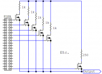
Consider attached drawing.
I have pondered over using an FPGA with a lot of outputs, some randomness (as seen by a dCs) + a couple of levels (say 4-24 units per bank, 2-4 levels in total). I never had the courage to start learning FPGA programming - but only having to modify a project is another kettle of fish altogether
I would expect switching at MHz interesting
Output stage is for demonstration only. JFET's and matched current sources are probably cheaper than ultra-precision resistors.
Let me know what you think
Petter
Consider attached drawing.
I have pondered over using an FPGA with a lot of outputs, some randomness (as seen by a dCs) + a couple of levels (say 4-24 units per bank, 2-4 levels in total
). I never had the courage to start learning FPGA programming - but only having to modify a project is another kettle of fish altogether I would expect switching at MHz interesting
Output stage is for demonstration only. JFET's and matched current sources are probably cheaper than ultra-precision resistors.
Let me know what you think
Petter
Attachments
Hi,
I am very interested in the design, but I would like to make a suggestion. With a platform like this it would be very easy to make multiphase output stage. Advantages of such approach can be seen in the following US patent applications:
20020053945 (Bruno Putzeys, Philips) and
20030095013 (John Melanson, Cirrus Logic)
So I suggest a minor modification to the modulator board:
Expand output stage I/O header from 20 to 40 pins (I suppose every other pin on header is GND.) Therefore it would be possible to drive more phase shifted output stages in paralell with lower per phase frequency and corresponding lower distortion due to timing errors. It would also make possible to use 80 pin parallel ATA (hard disk) cable with extra 40 ground wires and greater timing fidelity to connect to the output stage.
Best regards, Jaka Racman
With a platform like this it would be very easy to make multiphase output stage. Advantages of such approach can be seen in the following US patent applications:
Hi, this is very interesting. Do you where we could find information/papers on those patents?
On the hardware side, there are still a lot of pins available on the connector between the fpga board and the output stage. It would be easy to design a different output stage board with two TAS5112 chips and run them with different PDM signals. You could also use two seperate output stage and hook them to different header connector on the fpga board.
Regards,
David
DAX Group
Hi,
patent applications can be accessed at US Patent Ofice http://appft1.uspto.gov/netahtml/PTO/search-bool.html .
Just type in patent application number. To access images you will also need tiff viewer http://www.uspto.gov/patft/help/images.htm .
Regarding proposition for 40pin header it was more in direction of signal fidelity than in the number of the I/O pins, since I realised you have 79 I/O pins on 4 20 pin headers. I have some expirience with analog multiphase class D amplifier that had modulator and power stage connected by 40cm ribbon cable. Although every second wire was GND, I had some noise from power stage coupled back to modulator board. Result of this jitter was relatively noisy amplifier. Multiphase designs are particularly susceptible to noise because you have two stages switching at the same time with zero input signal when using even number of phases. This is why I use LVDS transmitters and receivers together with CAT5 cable in my next amplifier design (still in very early stage). I thought of using 3 TAS5015 modulators each fed with its own SRC1942 from the common input signal. I would then phase shift LR clock of each TAS5015 and then hopefully have phase shifted PWM signals. But I would give all that up in favour of DAX.
Best regards, Jaka Racman
Can't wait to see it!
This looks very appealing. I have been waiting a very long time to build a DIY DSP engine... if you want to hear the story, read on, if not skip to my comments at the end.
I first concieved of a DIY DSP project way back in 1998, still a 2nd year EE student. I did the first rough board design using Analog Devices ADSP-21060 DSP. It was of course, not a very good design, and too expensive with low-latency SRAMs and heaps of discrete logic. It featured the CS8412 DIR with an AD1890 for SRC functions, CS4390 DACs, and a PIC micro to handle front panel display, reset, user input, etc. I never built it thankfully, it would have been hell to debug, and I doubt it even would have worked properly. Worse, I couldn't get dev tools for the SHARC! But a second opportunity to make it a reality came up a few years later...
My graduation project for April 2001 was an audio DSP board centered around the much friendlier ADSP-21065L SHARC chip. This processor has I2S in/outs. I changed input/SRC to AD1892, and DACs to PCM1702 with a big analog output circuit. Although the 4 layer board design was complete, the availability of some key parts and free or cheap development tools for the SHARC processor prevented me from ever building it and getting it working... and that was the end of that. At least I got credit for it.
Since 2001, I've been working full time, but I've kept the project alive in my head, waiting for the break I needed to make it work. The board architecture has evolved a lot... first removing the DIRs, DACs and analog output stages so they could be put on separate modules and interchanged. I upgraded from AD1892s (integrated DIR/SRCs) to AD1896 SRC chips when they came on the market. Having all I/O modules off-board makes possible many new options like LVDS receiver boards for I2S directly from hacked consumer equipment, or a separate SPDIF/IEC958 board, or a separate module with a PMD-100 HDCD decoder from an old CD player, or, or... Of course all these interchangable modules required flexibility that discreet logic couldn't handle, which led me to add an FPGA as a configurable I2S mux and data reformatter. I replaced the PIC micro with a more useful Atmel AVR. Only recently have affordable, powerful FPGAs and free dev tools arrived on the scene with enough gates to do some real DSP with. Since free dev tools for the SHARC are still not available, it seems only natural to eliminate the troublesome SHARC at last (I still hold a grudge against AD for not releasing free dev tools, or at least a worthwhile educational package).
So I've been anxiously waiting 5+ years to make this a reality, and I've just been laid off from my company here in the Valley... hmm, what to do???
After I finish moving back to Canada, I'll have lots of time on my hands unless I find a new job right away, and I am looking to brush up my Verilog skills. I'd really love to get my hands into this project, doing a board spin and/or code development. Since a digital power amp isn't really a goal for me, my primary interest would be adding other DSP functionality, such as DSD->PCM conversion, and audiophile-grade IIR and FIR filters for tone control / speaker crossovers etc. that users could apply in standard DAC designs and so forth.
So a few questions for the DAX group:
1. What language are you using? VHDL or Verilog?
2. What input word width and sample rate are you using?
3. How soon can you get this puppy ready for us to sink our teeth in!?
This looks very appealing. I have been waiting a very long time to build a DIY DSP engine... if you want to hear the story, read on, if not skip to my comments at the end.
I first concieved of a DIY DSP project way back in 1998, still a 2nd year EE student. I did the first rough board design using Analog Devices ADSP-21060 DSP. It was of course, not a very good design, and too expensive with low-latency SRAMs and heaps of discrete logic. It featured the CS8412 DIR with an AD1890 for SRC functions, CS4390 DACs, and a PIC micro to handle front panel display, reset, user input, etc. I never built it thankfully, it would have been hell to debug, and I doubt it even would have worked properly.
Worse, I couldn't get dev tools for the SHARC! But a second opportunity to make it a reality came up a few years later...My graduation project for April 2001 was an audio DSP board centered around the much friendlier ADSP-21065L SHARC chip. This processor has I2S in/outs. I changed input/SRC to AD1892, and DACs to PCM1702 with a big analog output circuit. Although the 4 layer board design was complete, the availability of some key parts and free or cheap development tools for the SHARC processor prevented me from ever building it and getting it working... and that was the end of that. At least I got credit for it.
Since 2001, I've been working full time, but I've kept the project alive in my head, waiting for the break I needed to make it work. The board architecture has evolved a lot... first removing the DIRs, DACs and analog output stages so they could be put on separate modules and interchanged. I upgraded from AD1892s (integrated DIR/SRCs) to AD1896 SRC chips when they came on the market. Having all I/O modules off-board makes possible many new options like LVDS receiver boards for I2S directly from hacked consumer equipment, or a separate SPDIF/IEC958 board, or a separate module with a PMD-100 HDCD decoder from an old CD player, or, or... Of course all these interchangable modules required flexibility that discreet logic couldn't handle, which led me to add an FPGA as a configurable I2S mux and data reformatter. I replaced the PIC micro with a more useful Atmel AVR. Only recently have affordable, powerful FPGAs and free dev tools arrived on the scene with enough gates to do some real DSP with. Since free dev tools for the SHARC are still not available, it seems only natural to eliminate the troublesome SHARC at last (I still hold a grudge against AD for not releasing free dev tools, or at least a worthwhile educational package).
So I've been anxiously waiting 5+ years to make this a reality, and I've just been laid off from my company here in the Valley... hmm, what to do???
After I finish moving back to Canada, I'll have lots of time on my hands unless I find a new job right away, and I am looking to brush up my Verilog skills. I'd really love to get my hands into this project, doing a board spin and/or code development. Since a digital power amp isn't really a goal for me, my primary interest would be adding other DSP functionality, such as DSD->PCM conversion, and audiophile-grade IIR and FIR filters for tone control / speaker crossovers etc. that users could apply in standard DAC designs and so forth.
So a few questions for the DAX group:
1. What language are you using? VHDL or Verilog?
2. What input word width and sample rate are you using?
3. How soon can you get this puppy ready for us to sink our teeth in!?
Interested!
Actually, like the previous poster, I had this idea some time ago, 1995 to be exact. Needless to say I quickly found it impossible to realize at the moment but ever since then it's been lurking in the back of my mind as something that is indeed possibe but just too much work/too costly for a single person.
And now it's here!
I can only second the opinion of the previous poster and say: Let's get on with it.
Regards,
Magnus
It's free: Look
jwb said:It's true you can't get the dev tools for SHARC except 90-day evaluations and lots of money. But is the situation actually different for FPGA dev tools?
Yeah, Xilinx's free tools are pretty great.
Unfortunately unless you're up for designing a DSP/processor core from the ground up as state machines/logic it won't get you very far
Opencores HAS made some good progress with basic FIR and IIR filters and a few embedded microcontrollers, maybe some progress could be made?
All of opencore's stuff is GPL'd or LGPL'd, which is really cool. But if you use them and distribute your design in any way be sure to read up on them so you are aware of your responsibilities under the license.
 Awful quiet on this thread lately... must be final exam time.
 So a few questions for the DAX group:
1. What language are you using? VHDL or Verilog?
2. What input word width and sample rate are you using?
3. How soon can you get this puppy ready for us to sink our teeth in!?
We coding in VHDL. The input word width is only dictaded by the input stage (CS8416 and SCR4193), this means it supports 16, 20 and 24-bit.
At this moment we are putting all our time in producing the user manual which will answer 98% of potential questions and (you guessed right) on our final exams and projects. Unfortunately, we cannot predict production time as it will be function of the number of people willing to invest in the project. Judging by the feedback we received so far, we are hoping to start producing something as early as possible in 2004.
Gabriel,
DAX Group
very good project! CONGRATULATIONI'm very interested by this project, I've been searching, for 8 months, on all french forum to find a schema or an other guy who has already built this type of amplifier. But nothing.
And now I find your project, it's in english but I try to understand and to write. But my project was builting a Multichannel digital power amplifier (for my home cinema) as good as or better than the Bel Canto Evo 6. With your project it's not possible because your module has just a digital input and the pre-out from my pre- amplifier or all analog. This is the problem, if Ihave to put 6 DAC or ADC between my pre-amplifier and my "Multichannel digital power amplier" it will be very expensive!
That why a few times,seeing if other people or interested by this Multichannel D.P.A. and seeing if some very experiment people (Brian Brown or you) could suggest some answer and schema.
Thanks a lot if you can understand my english and if you can find a solution for the HI END Multichannel D.P.A.

But my project was builting a Multichannel digital power amplifier (for my home cinema) as good as or better than the Bel Canto Evo 6. With your project it's not possible because your module has just a digital input and the pre-out from my pre- amplifier or all analog.
As you said, our system has one digital input (coax or optic). However, as we said, the hardware is very flexible and adding one or multiple analog inputs is pretty straightforward. Most ADCs output I2S data at 192khz (the same type of data already being fed to the fpga), so one could simply duplicate the existing logic in the fpga to have more audio channels. In the same fashion, more output stages could be added.
In fact, adding an analog input is one of our next priority, since it makes the amplifier much more versatile and we still have a lot of analog recordings
And by the way, if it can encourage you, nous parlons tous francais...(french is our first language).
Rgds,
DAXgroup
- Status
- This old topic is closed. If you want to reopen this topic, contact a moderator using the "Report Post" button.
- Home
- Source & Line
- Digital Source
- A high-end digital amplifier for everyone