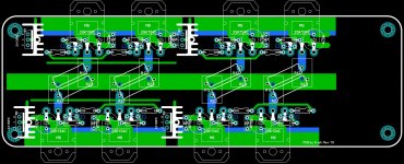
Assumption is the green traces are on the back/solder side, components are mounted on the top side.
Would have to be, how are you to solder under components, like the trim pots for example, if the traces are on the top side!
I have seen many layouts, in that the zobel network return path to the common point ground, use a separate conductor and not use the same return path, as the big filter caps occupy.
Why is it only a single sided pcb? Is there a cost advantage or are you making it yourself? I see that the mounting holes show like they have a via ring around them, why is that, when it is a single sided pcb?
What method is used for the Power bjt attachment to the heatsink?Are they mounted on the backside, but shown on the top silk/assembly.
ecap polarity symbol (+), on the top silk screen layer, should be on the outside of the circle. That way you can see orientation(inspection) when the component is soldered into place.
Not sure if the graphics represent the top silk scrwen layer or the top assembly layer or are they the same? Looks to be silk, so you really don't want the component to hide the silk info. Silk is used for both assembly and troubleshooting.
Add copyright and date.
The component placement looks very good, thus makes a nice layout.
Okay enough review for now, see what you think of my feedback so far and what others think
Take care
Rick
Richard,
I am not a pcb fabrication expert, but this my understanding of the process.
If you have PTH holes, it means it is a two sided pcb. Thus you must have a pad on the bottom side to have an annular ring. I do not know of fab shop that will plate holes that do not have some sort of annual ring. So if you have now established that the pcb is 2 sided, make good use of it and add traces, planes etc to the bottom side.The stock material is double sided Cu cladding to begin with.
If it is only a one sided pcb, stock material only has Cu cladding on one side, drilling is done after etching. There is no plating process used in this case.
I guess the definitive answer it ask a pcb fab house what their capabilities are.
All my pcb fab design manuals, do not even mention single sided fab, as it only used for very low cost pcb's, using low component density. I will look around today to see if I can come up with more information on this subject.I have some old IPC manuals that may cover this subject.
Last edited:
yes tiz all true. You would have to use a two sided pcb. But still have signal trace access on top side.
myself? glad you asked. i use 2 sided and have wide ground plane under only the DC rails.
I do it this way only when experimenting and more likely than not - will think of something else later and dont want to make a whole new pcb to incorp the new idea/part. Its just easier on the DIY'er and experimenter.
As for performance, it does not improve anything. You can take a look at my headphone amp forum and see my pcb layout to better descibe in a picture what a thousand words cant convey. Then apply to this great project or modify as you see fit to do. Its only a suggestion for those of us who constantly build and tinker with things...
Thx- Richard
Hi Richard and others,
P.S. Am I the only one doing a layout review of what has been proposed, rather than describing the pcb fabrication process.
Cheers
Rick
Well, I guess that depends on the application. Great many audio products in the past and probably presently use single sided pcbs for cost reasons most probably. Double sided/muti-layer pcb's extra cost probably do not justify the extra expense for these products.As for performance, it does not improve anything.
Sure I can, I am always open to ideas to learn from. I can show you some layouts as well, if you are interested. I have done quiet a few of them in my time and continue to do them for my own home projects.You can take a look at my headphone amp forum and see my pcb layout to better describe in a picture what a thousand words cant convey.
I do understand your reasoning for the intended application of having some thing that is easy to modify, thus the layout technique that you describe. Pcb's are expensive, especially at the proto stage where quantities are small, so having the biggest bang for the buck, is always good use of ones $.Then apply to this great project or modify as you see fit to do. Its only a suggestion for those of us who constantly build and tinker with things.
P.S. Am I the only one doing a layout review of what has been proposed, rather than describing the pcb fabrication process.
Cheers
Rick
Last edited:
Is this a acceptable layout...
As I already commented, I think there are reasons to use a wider layout with the OPS all on one side.
Any reason not to use such a layout?
Best wishes
David
When all of the OPS devices are on one side, the board tends to be longer than 10" which I like to stay below on laser printer DIY transfers. Especially beyond 3 or 4 pairs. No other big difference, but I lean on Dual in line. I think it cares over from my DIP red and blue tape adventures years ago. Shucks I revealing my aged dementia thoughts and such.
thoughts and such.... than 10" which I like to stay below on laser printer DIY transfers. Especially beyond 3 or 4 pairs...
Most laser printers will do A4 or US 13" paper which should allow 6 or more pairs.
Seems a reasonable limit but I haven't tested it yet.
On the PCB from post #180 it looks like all the OPS on one side would make the board no wider any way.
I understand habits to do it one way but I think the "across" the symmetry axis is a little better for thermal and layout.
Best wishes
David
I have never seen transfer paper that is 13" long.
The thermal aspect is a very important one. Do CFA have a sensitivity to thermal problems?
There are pro and cons on both sides of the aisle, maybe I will do both if time permits.
Dadod said he wanted separate grounds for the front and back ends too. That is easier to me in the symmetrical layout.
Well I had better put my computer in the Sprint Layout mode soon and have some fun. It might sound crazy to some, but doing layouts is fun and relaxing creativity to my mind and soul. All thanks to Alex MM, he is my leader and has been very helpful over time. Thanks Alex. I just try poorly to do what you do so well.
The thermal aspect is a very important one. Do CFA have a sensitivity to thermal problems?
There are pro and cons on both sides of the aisle, maybe I will do both if time permits.
Dadod said he wanted separate grounds for the front and back ends too. That is easier to me in the symmetrical layout.
Well I had better put my computer in the Sprint Layout mode soon
and have some fun. It might sound crazy to some, but doing layouts is fun and relaxing creativity to my mind and soul. All thanks to Alex MM, he is my leader and has been very helpful over time. Thanks Alex. I just try poorly to do what you do so well.RNMarsh, where is your Headphone Amp?
This will be a double sided board so may there can be some TEST points added for development.
Amplifiers -- Headphone systems - Marsh Headphone Amp from Linear Audio --- (now on page 2) page#302
-RNM
Last edited:
Great job so far. Looks like fun. I loved doing layouts, too.
I do not believe that it is a good idea to put the output resistor inside of the output inductor.
Are those disconnected copper "islands", at the top and bottom, under the leftmost output devices? You don't want any free-floating copper that isn't connected to anything.
I know that the following will seem to be "off the wall". But the caps that feed the output devices are directly providing the current that makes the music come out of the speakers. They ARE the signal path. (See the link in my signature section, below!)
Trace inductance, and therefore trace length between the caps and where the fast-changing high currents will be needed, is your enemy.
Instead of two big (10000uF) caps, it would give lower impedance to use smaller values in parallel, such as 2x 4700uF, or 3x 3300uF, or 5x 2200uF, or 10x 1000uF. (It might also be nice if you could star the output devices wrt the big cap, or star the power and ground rails to each device plus give each one its own 2200 uF or larger cap, plus some smaller ones.)
How were the 22uF values calculated, for the decoupling caps near each output device? I would use the largest value that can be squeezed in (certainly the largest value in that case size), or, even better, add a larger value in addition to the 22 uF (220 uF to 1000 uF), or, better yet, multiple smaller values in parallel. I know, you're out of space. But these could affect the transient response and imaging accuracy.
And the 100 nF caps are very far away from even the closest driver's collector pin! There should be one for each collector pin, right AT the pin if possible. A few extra millimeters from the pin can make a difference. They need to be very close, for HF stability. At high frequencies, the inductance of more than a centimeter (or probably much less) of PCB trace makes them almost totally useless.
Wow, a two-sided board would give so many better options for the layout. But if making them with a laser printer it can be difficult to get a good-enough alignment match for boards longer than six to eight inches or so (or at least it was with my old HP LJ 4).
Dadod said he wanted separate grounds for the front and back ends too. That is easier to me in the symmetrical layout.
I mean a symmetrical layout too.
Just that the ops is symmetrical "across" the axis, like a "T"
Rather than parallel to the axis, like your "U" shape.
Make sense?
Does anyone know of a layout like this to use as an example?
Best wishes
David
Would making a front end and separate OPS board be a prudent objective? Since the ground and voltages would be different anyway. Something like OStriper would do or did do. Then I could make a "Beast" similar to what he is doing on the GLA.
I was going to suggest that, too. It would also provide better layout possibilities.
I have a little concern about the gate protection zener diodes that, in an unfortunate event of output being shorted to GND, there could be large current going through them as well as through the driver transistors that may result in these devices being driven beyond their maximum limits and getting destroyed. Could this be a real issue?
IM very HO, this is truly evilWould making a front end and separate OPS board be a prudent objective?
There's loadsa issues but one thing this means is that 'real life' is even less likely to be reflected in SPICE world for important stuff like stability.
YMMV but I like my sims have some semblance to 'real life'.
- Home
- Amplifiers
- Solid State
- 200W MOSFET CFA amp