And battery supply?
I guess it is worse than good capacitor shunting (have not tried personally).
This circuit needs adjustments of R2, R3, R4 depending on rail voltages and on examples of VT1 and VT2. So, one must understand and "feel" how j-fets operate. The most important feature of this amp is related with your last question - why do we need those complications with excessive PS components.
I found this from listening experience - sound becomes crystal clear, if one does not allow signals to walk along PS chains - all voltages and consumed currents variations under signal must be stopped as close to active parts as possible. Therefore I use solutions based on VT3-VT4, and VT7. At this, simple capacitors shunting does not work well, active parts based solutions are better.
Hi,
I plan to follow your schematic but I have to wait for a long time for the parts. So with what I have in my hand, I come up with a schematic that I can build for testing. I made it like an preamp and test in my system. Do you think it is worth to test or I just need to wait for the parts and build the correct schematic?
Attachments
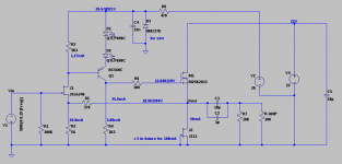
What means k392? 392 Ohm?
What Type are the Diode strings?
Yes, 392 Ohms. The diodes are red light LEDs.
Hi,
I plan to follow your schematic but I have to wait for a long time for the parts. So with what I have in my hand, I come up with a schematic that I can build for testing. I made it like an preamp and test in my system. Do you think it is worth to test or I just need to wait for the parts and build the correct schematic?
The input stage is OK, but output is not in line with my priciple (the load is in parallel to ACTIVE device). In your case it is parallel to current source. You should put p-channel MOSFET downside, and the CCS above it.
The input stage is OK, but output is not in line with my priciple (the load is in parallel to ACTIVE device). In your case it is parallel to current source. You should put p-channel MOSFET downside, and the CCS above it.
Thanks, I think I got it.
The input stage is OK, but output is not in line with my priciple (the load is in parallel to ACTIVE device). In your case it is parallel to current source. You should put p-channel MOSFET downside, and the CCS above it.
This is strange thing to say. The load is connected via caps to the output and parallel to both, CCS, and active device via power supply caps. I don't see an advantage in your configuration, could you elaborate?
This is strange thing to say. The load is connected via caps to the output and parallel to both, CCS, and active device via power supply caps. I don't see an advantage in your configuration, could you elaborate?
An answer is visible from your question - with the standard emitter (source) follower, everything contributes to output signal current (active device, PS caps, wiring to diode bridge when they conduct, wiring to transformer, trafo itself, etc.). With the standard approach, one gets standard "transistor" sound, with some better-worse variations. Just try my proposal - every stage is cut off the PS rails signal-wise by schematics, not only by caps. In this case I get what I like from sound (maybe it is only my preference). Very good sound is hidden in details, not in rough simulations.
I don't see an advantage in your configuration, could you elaborate?
This configuration renders the current draw from the supply constant, limited only by the output impedance of the current source. Thus the load-induced supply ripple should end up being a LOT lower than when the load's in parallel with the current source.
As Vladimir has pointed out this is a principle adopted by Andrea Ciuffoli and explained here : the Power Folllower
Yes I know that(I know about Cuiffoli buffer for log time), but is this supported with some real life measurement or it's just a subjective opinion?
All the Diode strings?
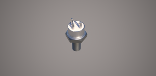
Do You have a mechanical Definition for the FET? I want to define it for my Library!
Thanks Vladimir...
Other diode strings are zeners, just select and adjust for voltage needed. The lowest noise/voltage ratio is for 5...7V zeners, typically.
The notion for mosfet kind, is used in wikipedia, it is not specially mechanical term:
"If the MOSFET is an n-channel or nMOS FET, then the source and drain are "n+" regions and the body is a "p" region. If the MOSFET is a p-channel or pMOS FET, then the source and drain are "p+" regions and the body is a "n" region. The source is so named because it is the source of the charge carriers (electrons for n-channel, holes for p-channel) that flow through the channel; similarly, the drain is where the charge carriers leave the channel."
Last edited:
Hello Vladimir,
do you have a datasheet of the KP903B?
Regards,
Jean-Paul
Dimensions of the transistor are on post 1..
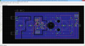
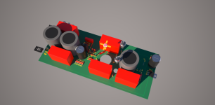
Hello Vladimir,
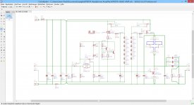
here is my contribution. I sent schematics and layout for comments and check.
The rendered view is how it should like: make this design accessible for anyone, ok, the parts needs to be available! Happy to use russian parts.
Regards,
Jean-Paul
here is my contribution. I sent schematics and layout for comments and check.
The rendered view is how it should like: make this design accessible for anyone, ok, the parts needs to be available! Happy to use russian parts.
Regards,
Jean-Paul
Attachments
Hello Vladimir,
here is my contribution. I sent schematics and layout for comments and check.
The rendered view is how it should like: make this design accessible for anyone, ok, the parts needs to be available! Happy to use russian parts.
Regards,
Jean-Paul
Thanks a lot Jean-Paul for your interest and contribution. However, I would not pay too much attention just to this low wattage schematics. Seems, similar schematics with triple-bjts at output are more attractive, in my other threads.
- Status
- This old topic is closed. If you want to reopen this topic, contact a moderator using the "Report Post" button.
- Home
- Amplifiers
- Solid State
- 1W SE Class A – Powerful Headphone or Weak Power Amp