Hello Diyers
Can anyone one have AX-14 amp one pair Pcb layout file of Sprint lay6 or Garber file. I lost my file from my pc.
Please help
I have this sprint file.
Attachments
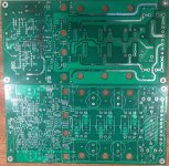
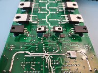
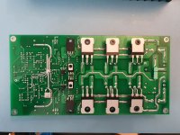
I received A40 boards from PCBway. Looks like an older version.
Is it the same circuit as the new version with a different layout?
Is there a BOM for this version?
Thanks in advance!
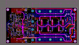
Add: Pic of board. The components are numbered but no values.
Attachments
Last edited:
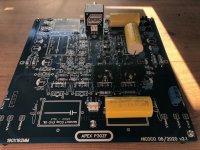
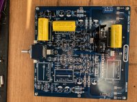
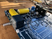
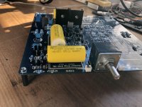
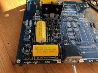
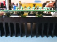
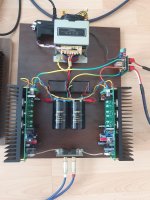
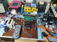
P30ZF allmost ready.
The left side is allmost stuffed and soldered, waiting on the last parts 2n5401 and 100uf, should arrived this week.
I will powering up soon.
The left side is allmost stuffed and soldered, waiting on the last parts 2n5401 and 100uf, should arrived this week.
I will powering up soon.
Attachments
I received A40 boards from PCBway. Looks like an older version.
Is it the same circuit as the new version with a different layout?
Is there a BOM for this version?
Thanks in advance!
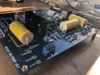
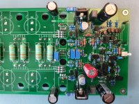
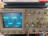
Hi. It's modificated version by my friend. This board has no ground loops and shows better values on spectogram. If I find the schematic will post it.
Add: Pic of board. The components are numbered but no values.
Hi, I attach the schematic here.
C9, R49 are optional. Use them only if you have spectrum analizer to set them.
For R50 use wire bridge.
I strongly recommended to use KSA1381/KSC3423 in VAS instead of NJE350/350 for better OLG and 10db better THD.
Attachments
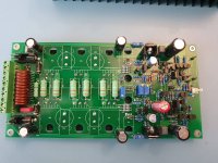
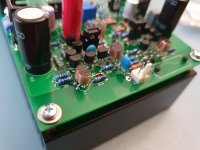
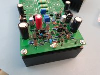
And some pictures:
Attachments
-
 viber_image_2020-06-05_20-22-37.jpg241.8 KB · Views: 279
 -
 viber_image_2020-06-05_20-22-30.jpg199.2 KB · Views: 236
 -
 viber_image_2020-06-05_20-22-25.jpg213.7 KB · Views: 266
 -
 viber_image_2020-06-05_20-22-20.jpg256.5 KB · Views: 662
 -
 viber_image_2020-06-05_20-22-15.jpg245.3 KB · Views: 684
 -
 viber_image_2020-06-05_20-22-09.jpg246.8 KB · Views: 708
 -
 Ku-F.png56.3 KB · Views: 730
 -
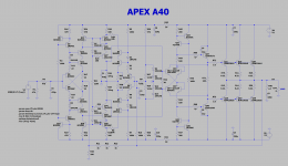 apex.png183.3 KB · Views: 758
Looks very nice, can you share files/gerbers with us ?The left side is allmost stuffed and soldered, waiting on the last parts 2n5401 and 100uf, should arrived this week.
I will powering up soon.
Thanks
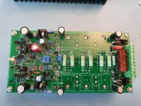
Other pics of the Amp.
Attachments
Yes i will !!Looks very nice, can you share files/gerbers with us ?
Thanks
@ Itco,
https://www.diyaudio.com/forums/att...amplifier-viber_image_2020-06-05_20-22-09-jpg
Did you solder on top of the solder mask or was there a way to avoid to have the mask on specific traces?
In the second case where did you order your board from?
https://www.diyaudio.com/forums/att...amplifier-viber_image_2020-06-05_20-22-09-jpg
Did you solder on top of the solder mask or was there a way to avoid to have the mask on specific traces?
In the second case where did you order your board from?
@ r_jik45
I ordered the PCBs in JLCPCB.
I open the solder mask on the high current planes and tracks, and also for the star ground connections. After that i add tin in the open places.
To add solder mask opens there is two ways in altium. The first one is manual draw (place line) in topSolder or bottomSolder layer and draw on the tracks. The second way is to sellect track and from propperties add manual Paste Mask Expansion width.
Attachments
Last edited:
- Home
- Amplifiers
- Solid State
- 100W Ultimate Fidelity Amplifier