thank you , my friend .
you're right !
So , the pic is wrong too ....
I must to check for other errors
that is the only one error in pcb
I`m ready whit PCB soldering to AX14 . I set BIAS at 100mA .
It`s work and sound great !
Now i want to test whit SMPS power supply .
For this case i try to make PCB .
You can see it here :
http://www.diyaudio.com/forums/power-supplies/253901-220-2x50v-whit-ir2153-pcb.html
I want to ask someone with experience for his opinion .
Regards !
It`s work and sound great !
Now i want to test whit SMPS power supply .
For this case i try to make PCB .
You can see it here :
http://www.diyaudio.com/forums/power-supplies/253901-220-2x50v-whit-ir2153-pcb.html
I want to ask someone with experience for his opinion .
Regards !
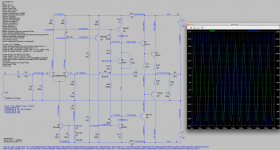
Posting an ltspice simulation of the AX11, with the models file that I used with it, which contains a few extra models I used and planned to test with.
I only ran the basic sims so far and checked phase margin with a tian probe. The phase margin looks fine at nearly 50degrees.
There is an issue with the bias spreader. I couldn't get models for the BD249C/50C and MPSA13, so I use TIP35C/36C instead of the BD and the BD681 instead of the mpsa. Using the BD681 may in part be a reason for the bias issue, as it is a good 700mA as is, but in any case, the spreader would require a trimmer to adjust it down some, unless someone wants (with a beefy heatsink) close to class A bias.
I added almost 5k6 in series with the 4k7 lower resistor in the spreader, to bring the bias down to about ~100mA. Still somewhat high, but more practical and less dangerous if the heatsink isn't very big. This means a trimmer should be something like 8k2 or perhaps 10k multi-turns.
Bandwidth is quite wide, nearly flat to some 100khz, and I didn't notice any signs of oscillations, however the thd is a little high at the lower end and climbs quickly above 1k, and gets quite high at the high end at 20khz. The sine wave looks more like a triangle at 20khz. This translates into close to 6% thd.
I would have to find better models, but still, as it is, it could use some tweaking to get it better behaved.
Attachments
Posting an ltspice simulation of the AX11, with the models file that I used with it, which contains a few extra models I used and planned to test with.
I only ran the basic sims so far and checked phase margin with a tian probe. The phase margin looks fine at nearly 50degrees.
There is an issue with the bias spreader. I couldn't get models for the BD249C/50C and MPSA13, so I use TIP35C/36C instead of the BD and the BD681 instead of the mpsa. Using the BD681 may in part be a reason for the bias issue, as it is a good 700mA as is, but in any case, the spreader would require a trimmer to adjust it down some, unless someone wants (with a beefy heatsink) close to class A bias.
I added almost 5k6 in series with the 4k7 lower resistor in the spreader, to bring the bias down to about ~100mA. Still somewhat high, but more practical and less dangerous if the heatsink isn't very big. This means a trimmer should be something like 8k2 or perhaps 10k multi-turns.
Bandwidth is quite wide, nearly flat to some 100khz, and I didn't notice any signs of oscillations, however the thd is a little high at the lower end and climbs quickly above 1k, and gets quite high at the high end at 20khz. The sine wave looks more like a triangle at 20khz. This translates into close to 6% thd.
I would have to find better models, but still, as it is, it could use some tweaking to get it better behaved.
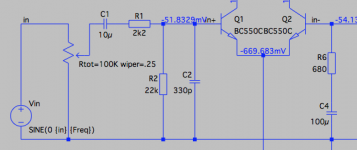
Use 33pF instead 330pF...
Use 33pF instead 330pF...
Ok, that works better, the sine wave now looks as such at 20k and thd goes down a bunch:
0.055584% @ 20 / 63.194W
0.068055% @ 1k / 64.234W
0.073453% @ 10k / 64.133W
0.132562% @ 20k / 63.827W
I only changed the miller caps and the bias was set at about 52mA in the outputs.
Phase margin goes down and perhaps a little lower than considered sufficient:
Measurement: phase_margin
step 1/(1-1/(2*(i(xlp:vinj)@1*v(xlp
 robe)@2-v(xlprobe)@1*i(xlp:vinj)@2)+v(xlprobe)@1+i(xlp:vinj)@2)) at
1 (-0.000155092dB,36.6357°) 559280
2 (-0.000155092dB,36.6357°) 559280
Measurement: gain_margin
step 1-1/(2*(i(xlp:vinj)@1*v(xlp
robe)@2-v(xlprobe)@1*i(xlp:vinj)@2)+v(xlprobe)@1+i(xlp:vinj)@2) at1 (30.0017dB,0.110819°) 6.16933e+06
2 (30.0017dB,0.110819°) 6.16933e+06
Gain margin is quite high, plenty of reserves, but it would be good to get a little higher phase margin.
I think higher gain transistors at the ips would probably help this some, I'll try that.
Switching to BC550C on the ips and its ccs brings down the phase margin further and the gain margin, although still high goes down as well. Only the phase margin becomes a cause for concern.
Measurement: phase_margin
step 1/(1-1/(2*(i(xlp:vinj)@1*v(xlprobe)@2-v(xlprobe)@1*i(xlp:vinj)@2)+v(xlprobe)@1+i(xlp:vinj)@2)) at
1 (-1.06514e-05dB,24.0798°) 697076
2 (-1.06514e-05dB,24.0798°) 697076
Measurement: gain_margin
step 1-1/(2*(i(xlp:vinj)@1*v(xlprobe)@2-v(xlprobe)@1*i(xlp:vinj)@2)+v(xlprobe)@1+i(xlp:vinj)@2) at
1 (25.9563dB,0.0911794°) 4.1425e+06
2 (25.9563dB,0.0911794°) 4.1425e+06
This also raised the bias current to about 99mA without adjusting it. I left it there, as this is still ok and may help thd some:
0.053246% @ 20 /63.215W
0.072522% @ 1k / 64.251W
0.071226% @ 10k / 64.152W
0.121024% @ 20k / 63.85W
The improvement, if any, is marginal.
Perhaps having a RL network on the output might help the phase margin.
Measurement: phase_margin
step 1/(1-1/(2*(i(xlp:vinj)@1*v(xlp
robe)@2-v(xlprobe)@1*i(xlp:vinj)@2)+v(xlprobe)@1+i(xlp:vinj)@2)) at1 (-1.06514e-05dB,24.0798°) 697076
2 (-1.06514e-05dB,24.0798°) 697076
Measurement: gain_margin
step 1-1/(2*(i(xlp:vinj)@1*v(xlp
robe)@2-v(xlprobe)@1*i(xlp:vinj)@2)+v(xlprobe)@1+i(xlp:vinj)@2) at1 (25.9563dB,0.0911794°) 4.1425e+06
2 (25.9563dB,0.0911794°) 4.1425e+06
This also raised the bias current to about 99mA without adjusting it. I left it there, as this is still ok and may help thd some:
0.053246% @ 20 /63.215W
0.072522% @ 1k / 64.251W
0.071226% @ 10k / 64.152W
0.121024% @ 20k / 63.85W
The improvement, if any, is marginal.
Perhaps having a RL network on the output might help the phase margin.
You can calculate the LTP source resistance at which distortion will double. Since Ib and Ic are proportional, Ib and Vbe as distortion mechanisms at small-signal are basically equivalent. Therefore, the total transresistance of the LTP divided by 1/Hfe gives you the source resistance at which THD will double, which is around 22k for the BC5xxC.
Total source resistance in this circuit is about 2.2k+680R, so Ib is not a dominant distortion mechanism. HOWEVER, if you use a 100k pot at the input, resistance will be 25k at half volume, which may double the THD.
So, does your simulation confirm my rough estimations?
Total source resistance in this circuit is about 2.2k+680R, so Ib is not a dominant distortion mechanism. HOWEVER, if you use a 100k pot at the input, resistance will be 25k at half volume, which may double the THD.
So, does your simulation confirm my rough estimations?
You can calculate the LTP source resistance at which distortion will double.
Using the current state of things as reference I assume.
Since Ib and Ic are proportional, Ib and Vbe as distortion mechanisms at small-signal are basically equivalent. Therefore, the total transresistance of the LTP divided by 1/Hfe gives you the source resistance at which THD will double, which is around 22k for the BC5xxC.
Interesting. I have been arranging the input filters in a different way to eliminate the effect of divider network that reduces the overall gain and inserting an extra resistor going to the base(s) on the ltp so it could be placed as close as possible to the base(s) to be more effective at HF.
Thus this would play in role in this calculation, however I haven't noticed the effect yet. I am certainly not looking at this properly, which is an opportunity to figure this out.
I've been arranging this into a pi network with the filter cap between the 2 resistors, and the other resistor of higher value being placed before that pi network and after the series dc filter cap.
Total source resistance in this circuit is about 2.2k+680R, so Ib is not a dominant distortion mechanism. HOWEVER, if you use a 100k pot at the input, resistance will be 25k at half volume, which may double the THD.
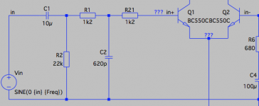
Would that be arranged as on that screenshot then?
I didn't put in a log pot there, as I may have this somewhere but haven't used it, so I put a lin pot.
This 2.2k+680 would be R1 + R4 then? And with a pot there, the part of it from the cursor and the input would be added to this sum?
Personally I would never insert any pots there at the input, I'd rather have a buffer or the direct output from a preamp, that would already be buffered and the volume adjustment be done before that. I always use mix tables and not hifi preamps to drive amps, so the volume is adjusted otherwise and there is no need to insert anything like a pot. Actually, most mix tables are heavily buffered on their outputs and have a dc blocking cap, so the one on the amp's input is too much.
So, does your simulation confirm my rough estimations?
I'll try a few things, however I'm not sure how to isolate this contribution, as the amp itself will have a different level of thd at different power level, regardless of how the input is driven.
Attachments
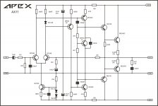
Whatamplifier was this based on? I ask, because the circuit appeared almost identical to an early Yamaha MX series.
It's the apex ax11. As is. Hardly changed, except for the different models because I couldn't get the exact ones called on by the schematic and also I added a resistor in the bias spreader to reduce the idle as it is high with the values on the schematic.
One added difference lately is to lower the miller caps from 330p to 33p, which changes things a lot, as the sine wave was ugly at 20khz.
Attachments
I just add a 25k resistor in series with the input. Maybe you designed the amp to clip at 1V input but you've got 2V input so the volume is at half? This is the worst-case scenario for source impedance.
The cap needs to be close to the base, it won't matter much where the resistor is, since there is plenty more in series with that resistor. Also consider how the corner frequency changes with pot position.
R1 and R6. It is useful to note that the base error current flows through the feedback resistor, not R6, but the effective source impedance for the feedback input is equal to R6.
Interesting. I have been arranging the input filters in a different way to eliminate the effect of divider network that reduces the overall gain and inserting an extra resistor going to the base(s) on the ltp so it could be placed as close as possible to the base(s) to be more effective at HF.
The cap needs to be close to the base, it won't matter much where the resistor is, since there is plenty more in series with that resistor. Also consider how the corner frequency changes with pot position.
This 2.2k+680 would be R1 + R4 then? And with a pot there, the part of it from the cursor and the input would be added to this sum?
R1 and R6. It is useful to note that the base error current flows through the feedback resistor, not R6, but the effective source impedance for the feedback input is equal to R6.
Having R1 (2k2) ahead of R2 (22k) divides the signal and the overall gain is only about 90% of the amp's actual gain. And there is no resistor that can be placed physically close to the base(s) at the ltp.
The cut off freq with R1 of 2k2 and C2 filter cap of 330p is about 219khz.
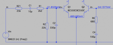
I arrange my input filters differently to avoid the divider effect and insert an extra resistor going to the lpt base(s) (see attached).
Using 1k2 for R1 and C2 becomes 620p for about the same cut off freq at about 214khz.
I put 1k2 going to the lpt base(s), but that coud go down to 1k to keep that same 2k2 total equivalent to what R1 was before.
On this ltp, but being a symmetrical topo, there are no degeneration resistors on the bases, so that new R21 can be placed very close to Q1's base, physically, which can help greatly in the hf (blocking).
Does this have any adverse effect that I haven't thought of?
The cut off freq with R1 of 2k2 and C2 filter cap of 330p is about 219khz.
I arrange my input filters differently to avoid the divider effect and insert an extra resistor going to the lpt base(s) (see attached).
Using 1k2 for R1 and C2 becomes 620p for about the same cut off freq at about 214khz.
I put 1k2 going to the lpt base(s), but that coud go down to 1k to keep that same 2k2 total equivalent to what R1 was before.
On this ltp, but being a symmetrical topo, there are no degeneration resistors on the bases, so that new R21 can be placed very close to Q1's base, physically, which can help greatly in the hf (blocking).
Does this have any adverse effect that I haven't thought of?
Attachments
Well, there is a far-reaching habit of placing resistors at transistor bases to improve stability, and this often happens in places where it's not needed or even has a negative effect by people who don't understand the mechanism.
The best place for a resistor of this kind is in series with C2, believe it or not. However I doubt it is needed or useful for this amplifier, and may worsen RF behavior if it is too large. I'm pretty sure the problem that resistor might solve would not happen with this amplifier, and it wouldn't be the best way of solving it even if so. The design has been tested and proven already, so I see no need to try and fix a problem that has not been shown to be in this design.
The best place for a resistor of this kind is in series with C2, believe it or not. However I doubt it is needed or useful for this amplifier, and may worsen RF behavior if it is too large. I'm pretty sure the problem that resistor might solve would not happen with this amplifier, and it wouldn't be the best way of solving it even if so. The design has been tested and proven already, so I see no need to try and fix a problem that has not been shown to be in this design.
I just add a 25k resistor in series with the input.
Ok, see attached, I'll run the same sims with that.
Maybe you designed the amp to clip at 1V input but you've got 2V input so the volume is at half? This is the worst-case scenario for source impedance.
I didn't design it
It's not clipping at 1V peak as is.
Here are the thd readings that I get with this extra 25k resistor, and the same 1.06V pk input source:
0.015559% @ 20 / 15.309W
0.015498% @ 1k / 15.538W
0.039853% @ 10k / 14.599W
0.117403% @ 20k / 12.345W
Bringing the input source voltage to double at 2.12V pk:
0.064853% @ 20 / 61.143W
0.066960% @ 1k / 62.058W
0.068122% @ 10k / 58.32W
0.109246% @ 20k / 49.327W
The effect that I think is more notable is not on the thd but rather the frequency response, which drops a lot more as frequency increases.
The cap needs to be close to the base, it won't matter much where the resistor is, since there is plenty more in series with that resistor. Also consider how the corner frequency changes with pot position.
It's clear to me that inserting a pot there at the input isn't a good idea.
I don't remember where I've read about this, but this was about inserting that resistor after that filter cap before the base. That would have a more effective action at blocking rf signals, and that resistor should be as close as possible to the base. Of course if there is that resistor there, the cap can no longer be close to the base, but the resistor can, and that's supposed to be good to block rf.
In any case, having everything very close and tight together with the shortest connections possible seems to be best practice.
R1 and R6. It is useful to note that the base error current flows through the feedback resistor, not R6, but the effective source impedance for the feedback input is equal to R6.
Would it be beneficial to attempt to equalize those impedance on both sides of the lpt?
Attachments
Well, there is a far-reaching habit of placing resistors at transistor bases to improve stability, and this often happens in places where it's not needed or even has a negative effect by people who don't understand the mechanism.
The reasons may not be exactly the same depending on where in the amp this is done.
I think the rf blocking at the input and output is needed to avoid issues, but once "inside" the amp, the reasons may be different.
The best place for a resistor of this kind is in series with C2, believe it or not.
So that would be more of a snubber than just a filter, similar to a boucherot/zobel network.
I bet this requires some more serious maths and isn't easy for ordinary diyers to grasp.
However I doubt it is needed or useful for this amplifier, and may worsen RF behavior if it is too large. I'm pretty sure the problem that resistor might solve would not happen with this amplifier, and it wouldn't be the best way of solving it even if so. The design has been tested and proven already, so I see no need to try and fix a problem that has not been shown to be in this design.
If there are minor things that can be done to improve the amp a bit, without adding complexity and too many parts, why not attempt it? Since it's being built by many, perhaps some might even try to improve the ones they've built.
I ran that sim with my rearranged input network. The changes brought down the phase margin a lot, to about 16 degrees. It wasn't quite sufficient before, but it is now lower. I tried it anyway and got slightly lower thd, but there were oscillations somewhere above 1khz, which didn't seem to add very much thd, but had to have some bad effect anyway:
RL=8 / Vin=.96Vpk / bias ~99mA / CM 33p
0.053399% @ 20 / 62.722W
0.055967% @ 1k / 63.773W
0.068334% @ 10k / 63.641W
0.114942% @ 20k / 63.246W
Then I added an output coil and tried various resistance values in parallel until the phase margin was much better. I stopped at 5ohms, although a slightly higher value would bring the phase margin even a bit better. However it's up to a bit over 41 degrees with that arrangement. The coil is 1uH, and I also reduced the miller cap to 27p.
Measurement: phase_margin
step 1/(1-1/(2*(i(xlp:vinj)@1*v(xlprobe)@2-v(xlprobe)@1*i(xlp:vinj)@2)+v(xlprobe)@1+i(xlp:vinj)@2)) at
1 (-0.000345855dB,41.2645°) 915620
2 (-0.000345855dB,41.2645°) 915620
Measurement: gain_margin
step 1-1/(2*(i(xlp:vinj)@1*v(xlprobe)@2-v(xlprobe)@1*i(xlp:vinj)@2)+v(xlprobe)@1+i(xlp:vinj)@2) at
1 (19.5625dB,0.0785516°) 3.60937e+06
2 (19.5625dB,0.0785516°) 3.60937e+06
Now there are no more signs of oscillations and thd went down a tad more.
CM 27p / output 1u // 5ohms
0.053396% @ 20 / 62.706W
0.055950% @ 1k / 63.758W
0.065181% @ 10k / 63.659W
0.113760% @ 20k / 63.364W
This should make it an overall more stable amp and the thd is a little lower than without those changes.
If one wants a little more phase margin, then increase a little the resistor in // with the output coil. I'm sure more small such things could be done to make it even better, without going all out changing everything.
RL=8 / Vin=.96Vpk / bias ~99mA / CM 33p
0.053399% @ 20 / 62.722W
0.055967% @ 1k / 63.773W
0.068334% @ 10k / 63.641W
0.114942% @ 20k / 63.246W
Then I added an output coil and tried various resistance values in parallel until the phase margin was much better. I stopped at 5ohms, although a slightly higher value would bring the phase margin even a bit better. However it's up to a bit over 41 degrees with that arrangement. The coil is 1uH, and I also reduced the miller cap to 27p.
Measurement: phase_margin
step 1/(1-1/(2*(i(xlp:vinj)@1*v(xlp
robe)@2-v(xlprobe)@1*i(xlp:vinj)@2)+v(xlprobe)@1+i(xlp:vinj)@2)) at1 (-0.000345855dB,41.2645°) 915620
2 (-0.000345855dB,41.2645°) 915620
Measurement: gain_margin
step 1-1/(2*(i(xlp:vinj)@1*v(xlp
robe)@2-v(xlprobe)@1*i(xlp:vinj)@2)+v(xlprobe)@1+i(xlp:vinj)@2) at1 (19.5625dB,0.0785516°) 3.60937e+06
2 (19.5625dB,0.0785516°) 3.60937e+06
Now there are no more signs of oscillations and thd went down a tad more.
CM 27p / output 1u // 5ohms
0.053396% @ 20 / 62.706W
0.055950% @ 1k / 63.758W
0.065181% @ 10k / 63.659W
0.113760% @ 20k / 63.364W
This should make it an overall more stable amp and the thd is a little lower than without those changes.
If one wants a little more phase margin, then increase a little the resistor in // with the output coil. I'm sure more small such things could be done to make it even better, without going all out changing everything.
Attachments
The resistor doesn't necessarily have anything to do with blocking RF, and I think there are much better ways of blocking RF if that is the goal. The resistor may be needed to prevent the amplifier from oscillating with certain source impedances. If not, then I think it should really be considered part of the stability compensation, as that is it's largest effect.
It could be that once, a person decided to try this resistor and found it made an audible improvement. Their inspiration was the "base-stopper" theory, so they may have assumed that was why it worked. However there are several effects this resistor may have, and each amplifier topology will have a different effect which is dominant, as well as differences that will occur due to implementation.
As far as having equal LTP source impedances, it can improve CMRR and PSRR by nulling the effect of C-B leakage on the LTP, if you don't use a cascode. It can sometimes lower the 2nd harmonic if the C-B leakage is not swamped by the other distortion mechanisms in the amp (or if the transistors have large Cob). However the input shunt cap causes an imbalance at RF, so you don't gain as much as you might hope, unless you make the cap very small. And you can't use an input pot because that will ruin the balance.
C2 lowers the impedance seen by the input.
Can you tolerate 470pF or 680pF?
Try 100pF and see if it gets even worse.
On the original ax11?
I increased C2 to 620p with R1 lowered to 1k2 to keep a similar cutoff freq. But I added another 1k2 between the cap and base of the ltp.
It could be that once, a person decided to try this resistor and found it made an audible improvement. Their inspiration was the "base-stopper" theory, so they may have assumed that was why it worked.
I can't recall exactly where I read about this, but I do remember that it was not some diyer and he was also into rf. The point was not just to have a resistor there, but rather the RC filter and a resistor being placed right at the base was the best and most efficient way to block rf. I couldn't fully understand the deep details of course, but I retained this as a possible trick to curb the effect of rf ingress.
I was curious to see what simply adding a sziklai pair on the ltp would bring, and with a few slight adjustments it works great and thd is one order of magnitude lower, with better phase margin and gain margin. One of the slight "adjustments" was to add a small cap (10p only) on the feedback resistor:
Measurement: phase_margin
step 1/(1-1/(2*(i(xlp:vinj)@1*v(xlp
robe)@2-v(xlprobe)@1*i(xlp:vinj)@2)+v(xlprobe)@1+i(xlp:vinj)@2)) at1 (-0.00050055dB,48.5508°) 2.85393e+06
2 (-0.00050055dB,48.5508°) 2.85393e+06
Measurement: gain_margin
step 1-1/(2*(i(xlp:vinj)@1*v(xlp
robe)@2-v(xlprobe)@1*i(xlp:vinj)@2)+v(xlprobe)@1+i(xlp:vinj)@2) at1 (12.4966dB,0.158476°) 8.97028e+06
2 (12.4966dB,0.158476°) 8.97028e+06
I also upped the value of the resistor to 10ohms in the R//L on the output.
Plenty more phase and gain margin.
And here's what thd looks like now:
RL=8 / Vin=.96Vpk / bias ~100mA
CM 47p / output 1u // 10ohms / Cfb 10p
0.006872% @ 20 / 62.968W
0.005680% @ 1k / 64.03W
0.004660% @ 10k / 63.923W
0.011176% @ 20k / 63.596W
And lastly, for the low end, I tried upping the C4 from 100u to 220u:
0.003802% @ 20 / 63.606W
0.004605% @ 1k / 64.031W
A bit more difficult to find and expensive cap for C4, an extra small one on the feedback and 2 small signals and resistors, and we get a much better result for few small changes.
Wouldn't that be better?
As far as having equal LTP source impedances, it can improve CMRR and PSRR by nulling the effect of C-B leakage on the LTP, if you don't use a cascode.
Is that something you make the effort doing in your designs?
Attachments
- Home
- Amplifiers
- Solid State
- 100W Ultimate Fidelity Amplifier