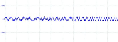
In the meantime, waiting for the next sim to be ready, I went back to at an earlier measurement that I made on one of both 8n2 caps with a DSD512 recording with a 4nsec sampling interval on a 1usec/div time base.
Spikes in this case are clearly visible, so It may be an idea trying to get similar spikes in my simulation.
Hans
Spikes in this case are clearly visible, so It may be an idea trying to get similar spikes in my simulation.
Hans
Attachments
Marcel,
is trying to force simulated spikes in the information stream not looking in the wrong direction.
What exactly is the difference when the .dsf file is made with a quasi multibit converter (QMC) instead of with a one bit PCM2DSD .
Isn’t that difference the amount of HF noise that is quite a bit lower with the QMC ?
When being processed by the Firdac’s shift registers, both versions will have to deal with the same spike problem, but after being filtered the QMC version doesn’t show the odd spectral lines caused by FM.
So seemingly not the spikes but the larger HF noise are causing this.
Should therefore not all the attention being given to the reconstruction filter instead of looking at spikes produced by the shiftregisters?
Hans
Hans,
Isn't it in reality more complicated than needing to focus in one single area? We could use a PWM modulator with a more powerful FPGA, for one thing. We could could use various strategies for a different type of output stage, etc.
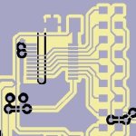
Changing the subject a bit and with regard to spikes, here is a section of the dac PCB surface:

I will describe a problem I found in a different dac-related circuit and a possible dilemma: Shift register bypass currents are forced through vias (bypass cap is C19, U7 is the shift register). IME, that causes more noise problems than if bypass currents are kept more on the surface layer. A decision was made to route the shift register signals on the surface, and to duck the bypass currents down through a lower layer. I'm not sure what would happen if the opposite strategy had been used, which would be to use solid surface fill under the shift register chip as a low inductance bypass current path. To do that would require ducking all the data signals down through a lower layer. Which approach would be worse in terms of shift register output noise? Well, one problem is that noise could be added to the data signals which are also the dac outputs.
Another possible approach to clearing up the fill area under the shift register might be to rotate the chip by 90-degrees and route the data signals around one end of it in sort of a Y-shaped path. Propagation delays would be longer, etc., but without trying it and or EM field simulation its not clear if there might be some solution to be found in that sort of way.
The above having been said, don't know offhand which strategy would be best/worst in the end. Again, its just that IME there can be considerable benefit to keeping bypass currents on the surface layer through a direct path.
Mark
Isn't it in reality more complicated than needing to focus in one single area? We could use a PWM modulator with a more powerful FPGA, for one thing. We could could use various strategies for a different type of output stage, etc.
Changing the subject a bit and with regard to spikes, here is a section of the dac PCB surface:
I will describe a problem I found in a different dac-related circuit and a possible dilemma: Shift register bypass currents are forced through vias (bypass cap is C19, U7 is the shift register). IME, that causes more noise problems than if bypass currents are kept more on the surface layer. A decision was made to route the shift register signals on the surface, and to duck the bypass currents down through a lower layer. I'm not sure what would happen if the opposite strategy had been used, which would be to use solid surface fill under the shift register chip as a low inductance bypass current path. To do that would require ducking all the data signals down through a lower layer. Which approach would be worse in terms of shift register output noise? Well, one problem is that noise could be added to the data signals which are also the dac outputs.
Another possible approach to clearing up the fill area under the shift register might be to rotate the chip by 90-degrees and route the data signals around one end of it in sort of a Y-shaped path. Propagation delays would be longer, etc., but without trying it and or EM field simulation its not clear if there might be some solution to be found in that sort of way.
The above having been said, don't know offhand which strategy would be best/worst in the end. Again, its just that IME there can be considerable benefit to keeping bypass currents on the surface layer through a direct path.
Mark
Last edited:
Mark,Hans,
Isn't it in reality more complicated than needing to focus in one single area? We could use a PWM modulator with a more powerful FPGA, for one thing. We could could use various strategies for a different type of output stage, etc.
Could be a next step, but first I'm just trying to find an answer to the question why QMC converted .dsf files do not show odd spectral lines and PCM2DSD do.
Same digital path, same shift registers, same spikes.
My preliminary view is that this can only be caused by the reconstruction filter because of the different HF noise content with PCM2DSD.
So far I could not get the added spectral lines appearing in a sim, but I just found an updated Spice model of the OPA2210, so who knows.
And also using more realistic 8.2nF input caps with serial inductance and resistance could help to make a difference.
Small problem is that every simulation takes many, many hours.
In the meantime I have made an alternative reconstruction filter with transistors that could be a solution.
But before showing this, it would be nice when I finally could succeed to replicate real life.
Hans
As I showed in post #2667 there are also simple 1-bit modulators that do not show spectral lines with this DAC. So same digital path, same shift registers, same output stage but different 1-bit modulators. One causes spikes, the other doesn't.why QMC converted .dsf files do not show odd spectral lines and PCM2DSD do.
Using vias with bypass capacitors is common practice.Shift register bypass currents are forced through vias (bypass cap is C19, U7 is the shift register). IME, that causes more noise problems than if bypass currents are kept more on the surface layer. A decision was made to route the shift register signals on the surface, and to duck the bypass currents down through a lower layer.
IMO what is questionable with Marcel's layout is that ground plane has slits beneath the shift registers. These may cause noise & reflections for critical signal traces above the slits. For HF traces return current path is beneath the signal trace. (second picture is from https://incompliancemag.com/alternative-paths-of-the-return-current).
Attachments
Is the FM the cause or the result from what’s causing it?FM-like intermodulation as Marcel suggested. In my tests modulator has by far the biggest impact on spectral lines. E.g. with PCM2DSD all output stages I've tested produce same spectral lines.
And yes, it’s obvious that it it is FM but where and why does it happen.
Not in the PCM2DSD, not in the Digital part of the RTZ Firdac, so it must happen at or after the node where the eight 3k01 resistors come together.
For getting FM you need more than a few resistors so to me the most likekely place is at the input of the first op-amp.
That’s why I think the input circuitry should not start with an op-amp.
Hans
P.s. your AK4493 had no problems with the PCM2DSD, right?
If so this converter does not produce the odd spectral lines and if it did it would show in the simulation.
Last edited:
Why do spectral lines happen? Probably in significant part because there is carrier energy to deal with.
In terms of how it looks on an FFT, we can make an unwanted signal look like noise, or make it look like a spectral line. It depends how the signal energy is distributed across the bins. Since we are looking at FR only and not phase response, we don't know how smooth or impulsive FFT "noise" may be, or even if it is quite deterministic (e.g. a sine sweep). We only know its not PSS if it doesn't make a spur (spurious/unwanted spectral line).
And of course one thing that makes spurs is PSS or PSS-like repetitive patterns produced by a modulator. IOW, its algorithmic.
Last edited:
Regarding via inductance, its usually the reason bypass caps are limited to no more that .1uf or .01uf. Any bigger than that tends to resonate with via inductance and cap self-inductance (usually vias account for a lot of the inductance). If we need 22uf bypass caps, then we might want to reconsider using bypass vias. Slowed bypass current propagation time also may increase transients in data signals.
Regarding signal routing complications, we might be better off with a 6-layer board.
On the subject of ground plane discontinuities under a digital signal, among other factors the amount of signal reflection depends on the highest frequency present in the risetime of the signal, and how much of the highest frequency signal's period is spent passing over the discontinuity, given the signal's propagation velocity. Also a small lumped discontinuity may be used for impedance matching in the steady state case. Doesn't mean there won't be some emissions if circuitry is unshielded, since there are always some emissions anyway. The usual concern is keeping emissions under regulated levels without requiring costly shielding mitigation, etc. Moreover, given this is a dac with a doubled clock, and given that dacs sometimes benefit from less than the fastest possible risetimes, at least we aren't dealing with frequencies as high as some PCB designers have to be worried about.
Last edited:
ThxThe DSF file I sent you was generated with sox-dsd with 8th order filter. So not a quasi-multibit modulator.
Not really. Parasitic inductance of 1206 ceramic capacitor is about 1nH. The via inductance of these 22uF capacitors is probably less than that.usually vias account for a lot of the inductance
As a rule-of-thumb discontinuities of ground plane under HF signal traces should be avoided. But nothing prevents you from making your own layout based on your views.
Understood. However in this case the ground pin of shift register is connected to the ground plane with a single via. The sum of the via inductances for the bypass current to flow is part of what resonates with the bypass capacitance to create a resonant circuit that causes bypass impedance to vary with frequency. At least that's the model people commonly seem to use.
Assuming the parallel vias at the bypass cap and the large capacitance holds the power pin of the IC pretty steady, it may be the ground pin that will be doing most of the bouncing around. It would presumably produce a common mode noise for the output stage to deal with.
Assuming the parallel vias at the bypass cap and the large capacitance holds the power pin of the IC pretty steady, it may be the ground pin that will be doing most of the bouncing around. It would presumably produce a common mode noise for the output stage to deal with.
Last edited:
AK4493 is a switched capacitor dac. So the lack of spectral lines with PCM2DSD does not say anything about how PCM2DSD (or any other modulator) works with this RTZ dac.P.s. your AK4493 had no problems with the PCM2DSD, right?
If so this converter does not produce the odd spectral lines and if it did it would show in the simulation.
When the spectral lines were created within the audio band during the conversion wihin the PCM2DSD algorithm, the AK4493 would faithfully reproduce them.
And when I’m right, this D/A is also driven with Ldsd, Rdsd and Bit Clock, just like the RTZ Firdac.
IMO this excludes the PCM2DSD from producing these spectral lines, but what it most likely does, is using a noise shaping algorithm that that is too aggresive for the used reconstruction filters with op-amps directy after the shift registers, where the AK4493 with a completey different topology has no such sensitivity.
That’s how I see it, but I’m trying hard to get a better foundation for this assumption
Hans

- Home
- Source & Line
- Digital Line Level
- Return-to-zero shift register FIRDAC