Ok, I see.OK, it was quicker to draw. My original connects feedback capacitors to ground. Today I would connect all through one DC blocking capacitor like on picture, and to hell with ground, truly balanced 😁 X
Similar to what they have in the TI application note.
Input offset current and voltage is not cancelled out though.
If you have each chip amp as differential it will take care of those.
Otherwise servo will help.
Attachments
You still need small caps to GND (or input reference) from either leg of the main DC blocking cap. Otherwise the circuit's common-mode gain is unity and thus very prone to oscillate.Today I would connect all through one DC blocking capacitor like on picture, and to hell with ground, truly balanced 😁 X
More importantly, the offset gain for the individual amps in each leg is the full signal gain which might give some surprises.
Hi KSTR,
Did you mix up my drawing #21 and those from #23 and 24?
I drove balanced in balanced out, the only difference from what I have working is removed ground in between feedback capacitor. Voltage in that place will still be 0 volt, so no unity gain.
Like this one can ground one imput and drive it unbalanced, balanced source is of course better.
@pbilous
You drove balanced line receiver circuit. This version has lot of sense for me if only single or parallel lm3886 is in use.
Even then strict care must be taken that input is connect before Amp is switched on, or negative input grounded. Otherwise negative input gets 100% feedback = unity gain, and lm3886 is not happy with that. Anyway, input must me connected to source of low impedance before powering up. This also rules out placing potentiometer at input.
When bridged chips are used, I think my version is more appropriate.
I was referring to the circuit in post #21.Hi KSTR,
Did you mix up my drawing #21 and those from #23 and 24?
I drove balanced in balanced out, the only difference from what I have working is removed ground in between feedback capacitor. Voltage in that place will still be 0 volt, so no unity gain.
Like this one can ground one imput and drive it unbalanced, balanced source is of course better.
Hi, OK, but I don't think anything more is needed on that diagram. Actually if we add input resistors (say 22 k) from inputs to ground + power decoupling capacitors, that's finished and ready to work.I was referring to the circuit in post #21.
It might even work, sort-of, but it is definitely not proper design.Hi, OK, but I don't think anything more is needed on that diagram. Actually if we add input resistors (say 22 k) from inputs to ground + power decoupling capacitors, that's finished and ready to work.
Amplifying the voltage offset difference between the amps in the same leg by a factor of 16 is not a good idea, and an unstable circuit isn't either. Also, the LM3886 is known to need some tricks to avoid oscillation even in an otherwise proper circuit (a shunt cap between input pins).
Hi, you could be right KSTR, I don't say I know everything 🥴.
But I didn't fully understand your explanation. Could you draw your recommended solution: balanced in, balanced out?
Picture speaks better 😁
When time comes I will take these modules out of my speakers and modify them. Then I can share measurements too. Would be great if we have optimal diagram for this by then
@pbilous
You drove balanced line receiver circuit. This version has lot of sense for me if only single or parallel lm3886 is in use.
Even then strict care must be taken that input is connect before Amp is switched on, or negative input grounded. Otherwise negative input gets 100% feedback = unity gain, and lm3886 is not happy with that. Anyway, input must me connected to source of low impedance before powering up. This also rules out placing potentiometer at input.
Most of these concerns are solved by adding unity gain buffer opamps in front of the LM3886.
Also for the paralleled chips in case they "fight eachother" in case of differing offset?Input offse currents are minimized because of differential configuration of the amp.
@stv ,
I also fully agree to that, offset DC between chips is another question do.
It would be great to measure DC offset of chips before pairing them into paralel, but this is quite labor intensive, dedicated rig would be required.
When I build these amps (remember from my first posts, all came from the same lot) I powered up whole lot without 0R1 load sharing resistors, then I measured DC offset and it was in few mV difference from each other.. That's safe. Also good share of pure luck.
I can imagine that difference can be in 10's of mV, then it will be wasting current in idle.. Trixy business as golum would say 😬
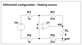
Let me start to show what goes wrong with your circuit.Hi, you could be right KSTR, I don't say I know everything 🥴.
But I didn't fully understand your explanation. Could you draw your recommended solution: balanced in, balanced out?
Offset: Let's say one amp has +10mV offset voltage (max as per datasheet), the other has -10mV. For DC both 1k (R2, R4) are connected but the center tap is open circuit. Because there is no DC blocker in between, the DC offset sees the full gain, in this case 320mV, or 160mV per current sharing resistor (not shown). Lets assume 0.1R then we get a whopping 1.6A of cross current, yikes :-(
Note: DC voltage of signal source outputs is zero, which is equivalent to the conditions within one of the legs of the BPA (Bridged Parallel Amplifier).
Adding a DC blocker between R2 and R4 reduces gain at DC to unity and hence 16 times less cross current worst case, 100mA.
Stability: I'm plotting the circuit gain at one of the outputs for both differential input voltage (blue) and common mode input voltage (green).
This time, I'm basically viewing from the perspective of the bridge action, not the parallel arrangement in each leg.
While the differential gain appears to behave nice and stable, the common mode gain shows extreme peaking (circuit will most likely oscillate). And that's for idealized conditions, zero part tolerances, and zero parameter difference for both amps -- all of which is of course completely impossible in real life.
Bottom line: The simple circuit, if working at all, has issues that make it completely unusable in practice.
------:------
What can we do? Basically follow TI's Appnote for the BPA, which isolates all the individual amp's gain circuits from each other and thus doesn't have stability issues.
Servos, with low-offset low-noise OpAmp and quality integrator capacitors with, if possible, 2% tolerance are the way to eliminate DC offset and provide a proper AC-coupling.
For a balanced input you add one of the known-good balanced input converter circuits of your choice.
There are no simple short-cuts... and please note TI's "detailed" schematic still only shows the concept in detail. Actually, you'd need to add a lot of stuff to make LM3886 behave. See this excellent resource https://neurochrome.com/pages/taming-the-lm3886-chip-amplifier from our local expert member @tomchr.
Actually, there's no way for you to know #1. Even if you buy all the ICs at one time from the distributor there's no guarantee they came from the same wafer or the same lot. Even if they did, there's also no guarantee that they came from two adjacent sites on the wafer. And two adjacent dice won't measure the exact same performance. Furthermore, two ICs mounted at different spots on the same heat sink will be subject to different temperatures, so they won't have the same performance even if they were identical. Sorry to burst your pipe dream, buddy....Three ways to optimize paralled LM3886:
1. Matching chip-amp ICs, ensuring that they are identical or come from the same manufacturing lot to minimize variations.
2. Matching the gain between each chip-amp, ensuring equal amplification across all branches of the circuit.
3. Optimize ballast resistors. These external resistors added to each chip-amp's output and balance the load for more equal distribution of the current.
")
#2 is pretty easy. ±0.1 % tolerance resistors are commonly available for not much money and even ±0.01 %, though not required, are not carved from solid blocks of rhodium plated unobtanium either. You do want to select resistors with a reasonably low voltage coefficient and temperature coefficient for the two gain setting resistors.
There isn't much to optimize for #3. The choice of ballast resistor is basically up to how much error current you're willing to let the LM3886es fight over. Recall that you get Gain*Vos at the output of each LM3886 and Vos can be anywhere in the ±10 mV range (says the spec sheet). So for a minimum gain configuration you may have 200 mV of offset voltage to contend with. This voltage is across two ballast resistors in series, so if you choose 0.1 Ω for those, you may get up to 1 A of current flowing, worst case. In most cases, more like 100 mA.
This is why I recommend that you run with unity gain at DC and the minimum (20 dB) gain within the audio band. That way you get only Vos at the output and the worst-case error current becomes Vos/Rballast. Much easier to handle.
If you increase the ballast resistors you burn more power in them and lose output power as result.
You'll want 10-22 uF || 0.1-1 uF bypass right by the LM3886es as well. I'm not saying that your circuit doesn't work, but if you push it with a 4 Ω load I bet you'll get a bit of parasitic oscillation as the output crosses about 32 V, peak.golden caps are just local decoupling
I've also found that if the V- supply, and thereby the mute pin, comes up before the V+ supply the parallel LM3886es can enter something that looks a lot like a soft latch-up condition. I don't know how much of an issue this is in practice, but I did see it in the lab. I chose to add a BJT that holds the LM3886es in mute until both V+ and V- are present.
Tom
I agree that it is impossible to match LM3886 ICs perfectly, but I feel way more comfortable ordering say 8 of them at once compared to just getting one by one from different places. Who knows if they were made 10 years ago or few months ago? And I would assume that nowadays the process for making them is at least in some ways better than 10 or 20 years ago.
In my build I have large NP capacitors between input unity buffers and INV/NON-INV inputs of LM3886 that serve a purpose of bringing DC gain of the amp to unity.
I measured Voffset at the output pin of each IC and I got -1.8mV -1.7mV 0.8mV and 1.1mV
for one channel for now.
In my build I have large NP capacitors between input unity buffers and INV/NON-INV inputs of LM3886 that serve a purpose of bringing DC gain of the amp to unity.
I measured Voffset at the output pin of each IC and I got -1.8mV -1.7mV 0.8mV and 1.1mV
for one channel for now.
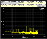
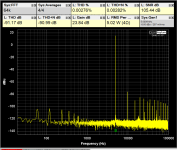
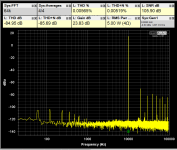
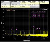
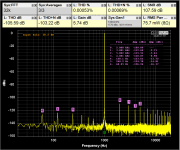
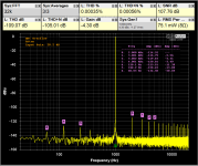
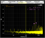
I made some new measurements with new settings and was able to lower the noise floor hence improving THD+N numbers.
8R results look very impressive.
Granted, mine is more of a brute force approach to reduce distortion by adding more chips in parallel. I recognize that at some point, such an approach will hit a point of diminishing returns where by adding more chips the distortion will not be reduced.
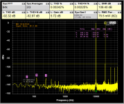
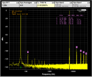
Attached are also IMDB measurements into 4R.
8R results look very impressive.
Granted, mine is more of a brute force approach to reduce distortion by adding more chips in parallel. I recognize that at some point, such an approach will hit a point of diminishing returns where by adding more chips the distortion will not be reduced.
Attached are also IMDB measurements into 4R.
Attachments
-
 5W_1khz_______scaled______8R.PNG40.5 KB · Views: 37
 -
 5W_10khz_______scaled______8R.PNG40.3 KB · Views: 34
 -
 50W_1khz_______scaled______8R.PNG40.5 KB · Views: 31
 -
 IMD1+5.5____scaled___4R.PNG34.9 KB · Views: 26
 -
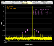 IMD18+19____10khz___30khz___4R.PNG32.9 KB · Views: 30
 -
 IMD60+7____scaled___4R.PNG35.1 KB · Views: 38
Last edited:
- Home
- Amplifiers
- Chip Amps
- Another LM3886 in parallel attempt - this time 4 of them!