Member
Joined 2009
Paid Member
This is a long thread, it sure would be helpful if we had a prioritized list - what's the #1 thing that would help the most, #2, #3. And is there much to be gained after that. I'm not putting this on Thor, just quoting what triggered off my thought. I have a single chip in my collection waiting for me to decide on how best to use it and I don't want to put in more time and effort than it's worth.Better focus on what helps most.
Thor
Indeed, hence why i'll make the dac by your schematic (i met a few people that either have cd-77 and cd-777, and consider them reference). I see everyone here in topic prefers simultaneous instead of i2s. And yours is i2s, have you changed your mind about that over the years? Logic part of the circuit is very simple in your schematic, i like it a lot for that, so i'd follow it to the letter, and since there is no output part, i'll leave that for experimentation as addon board. I'd only use usb input, so jlsounds i2soverusb board, clocks are on it, so difference would be to connect tda osc pins with appropriate cap value.Better focus on what helps most.
I spot something that might be of help. The lower JFET in the tube cathode is incrementing almost the exact about 13.5mA of current.
In reality J-Fets Idss varies from sample to sample. 2SK2394 is rated as 10mA - 20mA.
As HD depends on Transconductance, adding a P-Channel FET in a compound feedback pair would do more for less Iq than parallel J-Fets.
Then adding a folded cascode....
Thor
This is a long thread, it sure would be helpful if we had a prioritized list - what's the #1 thing that would help the most, #2, #3.
I actually wrote this before
https://www.diyaudio.com/community/...ate-nos-dac-using-tda1541a.79452/post-7546216
I have not tried some of the things, so no comments.
I see everyone here in topic prefers simultaneous instead of i2s. And yours is i2s, have you changed your mind about that over the years?
It was never tried. However given how the logic in TDA1541 works, I do not see any mechanism that would create a benefit, IF the inputs do not saturate. But I also see no drawbacks from simultaneous mode.
Logic part of the circuit is very simple in your schematic, i like it a lot for that, so i'd follow it to the letter, and since there is no output part, i'll leave that for experimentation as addon board. I'd only use usb input, so jlsounds i2soverusb board, clocks are on it, so difference would be to connect tda osc pins with appropriate cap value.
The AMR Circuit has a MCK input, it's marked CLK/174:
It reclocks all signals. There are also other clocks derived via CPLD (not shown) that are supplied, 174/6 & 174/3. These depended on sample rate, as the original design included Non-OS and 2X & 4X Oversampling.
174/3 & 174/6 are the TDA1541 DEM Clock and need to be opposite polarity, you pick the actual speed.
I would nowadays replace the 174 with a 574, it's "flow-through" layout if easier to implement a nice layout.
The Analogue Stage looked like this:
The 12AT7 is really a standin for 6072A, but these are too rare NOS to use in production.
Thor
Last edited:
Yes off course, I will check what Idss is for specific fatory spice model.In reality J-Fets Idss varies from sample to sample. 2SK2394 is rated as 10mA - 20mA.
As HD depends on Transconductance, adding a P-Channel FET in a compound feedback pair would do more for less Iq than parallel J-Fets.
Then adding a folded cascode....
But I am think that is more than 15mA? I will report that.
OK I can add folded cascode branch, but that will made topology a bit more complex, sure it will be interesting to have a look at these sims
Thanks.
While there may be additional parts, realistically speaking, folded cascode vs. normal cascode have the same number of active devices.
Core benefits include that the I/U conversion resistor is connected to "ground" not rail and can be arranged so that there is a bit of DC offset to bias a tube Follower as output stage, or a MOSFET or a J-Fet or even a J-FET plus P-Channel MOSFET Sziklai.
Other than the tube +/- 15V would do.
Thor
Core benefits include that the I/U conversion resistor is connected to "ground" not rail and can be arranged so that there is a bit of DC offset to bias a tube Follower as output stage, or a MOSFET or a J-Fet or even a J-FET plus P-Channel MOSFET Sziklai.
Other than the tube +/- 15V would do.
Thor
PS, filter is dimensioned for SAA7220B/C digital filter, tube buffer into 10k significantly increases H2 (over a J-MOS Sziklai) and instead of the adjustable resistor it really needs a servo, intentionally omitted, as are the active part numbers, they are not exotic, but all SMT.
SNR simulates 100dB unweighted.
SNR simulates 100dB unweighted.
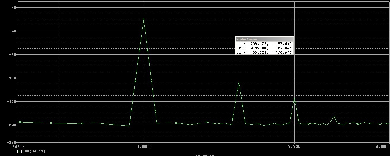
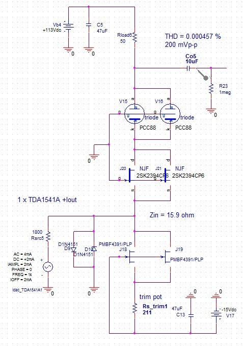
First some for IMHO optimum SE (JFET-Tube), with very low distortion, low output res, medium input res. But with "natural" harmonics transfer 
I put the PCC88 but it could be ECC88 and every other same type.
On the pic is for 200mVp-p as source for additional tube amplifing section and back the phase to 0deg.


I put the PCC88 but it could be ECC88 and every other same type.
On the pic is for 200mVp-p as source for additional tube amplifing section and back the phase to 0deg.
One interesting simple all jfet topology. With only 2 types of jfes in existing production. Again very good to excellent harmonics transfer and huge noise floor.
(Power for all devices is almost equally distributed so there is no overheating.)
Power supplies are +- 15V already present in TDA1541A...
With 4 times paralleled jfets in cascode modules, Zin is about 6.8ohms.
It is not sa problem to set 0mV Io input to dac at least in PSpice...
Zeners could be repaced with LEDs or Rs or something else...
Circuit behaves more less the same with 500 RIV for 2Vp-p output, only some voltage points should be corrected without much effort...
.
Note:
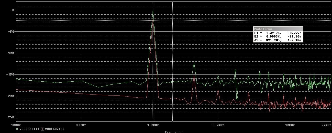
This FFT is from 10ms durtion and 0.1us step. Previous was with same dur. BUT with 1us step
.
I will post the version with a tube END biased from -15V power branch.
I used 1619 tube.

Note:
(Power for all devices is almost equally distributed so there is no overheating.)
Power supplies are +- 15V already present in TDA1541A...
With 4 times paralleled jfets in cascode modules, Zin is about 6.8ohms.
It is not sa problem to set 0mV Io input to dac at least in PSpice...
Zeners could be repaced with LEDs or Rs or something else...
Circuit behaves more less the same with 500 RIV for 2Vp-p output, only some voltage points should be corrected without much effort...
.
Note:
This FFT is from 10ms durtion and 0.1us step. Previous was with same dur. BUT with 1us step
.
I will post the version with a tube END biased from -15V power branch.
I used 1619 tube.
Note:
Attachments
The problem with today's jfets is too large deviations of Ids, for ten with the same Ids you need a considerable amount to match. I don't know how it is for the LSK170, but I used all the others that you mentioned and the differences could sometimes be more than about 5mA from the same batch.About the PSpice mdels for JFETs Idss values.
View attachment 1259627
I'm just now going to use the JFE2140 in my new amplifier with lateral mosfets, so I don't know what its deviations are but since it is not divided into grades, larger deviations are also possible because the Ids is from 12 to 23mA (at 25C). LSK389 (or LSK489) is already divided by grade so it would be an even better choice but also more expensive.
One BSS159 could replace 10 pieces or more 2SK3557-7, but according to some of my simulations THD and noise are higher in that case.
One BSS159 could replace 10 pieces or more 2SK3557-7, but according to some of my simulations THD and noise are higher in that case.
@grunf In that cascoded all-jfet-SE circuit it is not impotrtat so close match, than the ususal. because each branch can be set by own -PS CCS?
.
I will check tha same topoligies with JFE TI series, I think I have official PSpice models?
For all designs 2SK2394CP6 (CP7 is not in the production any more?) and BF861C are performing the best.
BF862 probably will perform so good but it is out of the production.
2N4391 (or in production SMD version with less Po) as final CCS is performing best for that position.
From the tubes, ECC88, PCC88 E88CC, rusian version, 6DJ8 are performing optimal.
Unfortuanatly 6MH5 is not performing well obtaining less than 0.5V of Vds for "lower" jfet...
Other very good tubes for this purpose I listed before, 5687, high trans pentodes in triode mode, probably some more we can find...
.
Try to make sound checl between MOS and J fets and it will be more clear? I would always use JFET. Probably even in the power supply rather BJT...
.
I have a huge lot of LSK170C i think? Measured and they very very consistant in Idss. First production samples.
.
One interesting double JFET could be of use
https://www.nxp.com/docs/en/data-sheet/PMBFJ620.pdf
by Philips. I have some and also i made a spice model so I will try to simulate...
.
I simulate a bunch of BJT IV circuits all of them (except 1-2 has very high distortion and bad niose floor WITH lower value of converted Voltages... So there are no room to use Tube gain stage after...
I will post that one I am going to make it is modified @Calvin version of simple BUT maybe the best IV. And "everythig" happening in the -PS branch so there is a direct conn to the -Ug for the tube
.
I will check tha same topoligies with JFE TI series, I think I have official PSpice models?
For all designs 2SK2394CP6 (CP7 is not in the production any more?) and BF861C are performing the best.
BF862 probably will perform so good but it is out of the production.
2N4391 (or in production SMD version with less Po) as final CCS is performing best for that position.
From the tubes, ECC88, PCC88 E88CC, rusian version, 6DJ8 are performing optimal.
Unfortuanatly 6MH5 is not performing well obtaining less than 0.5V of Vds for "lower" jfet...
Other very good tubes for this purpose I listed before, 5687, high trans pentodes in triode mode, probably some more we can find...
.
Try to make sound checl between MOS and J fets and it will be more clear? I would always use JFET. Probably even in the power supply rather BJT...
.
I have a huge lot of LSK170C i think? Measured and they very very consistant in Idss. First production samples.
.
One interesting double JFET could be of use
https://www.nxp.com/docs/en/data-sheet/PMBFJ620.pdf
by Philips. I have some and also i made a spice model so I will try to simulate...
.
I simulate a bunch of BJT IV circuits all of them (except 1-2 has very high distortion and bad niose floor WITH lower value of converted Voltages...
I will post that one I am going to make it is modified @Calvin version of simple BUT maybe the best IV. And "everythig" happening in the -PS branch so there is a direct conn to the -Ug for the tube
(I tried to test, before year or so, J108 (TO-92) version. It was huge Io with G and S connected to ground...
JFETs are imeadetly went to overhaeating so i stoped firture tests. I tried some Rs values but Io still was very high.
I didnt try to test with negative voltage on G.
Very good device, very low RdsON 8ohms, BUT it does not behave the same way in the simulations as in the real circuit...)
JFETs are imeadetly went to overhaeating so i stoped firture tests. I tried some Rs values but Io still was very high.
I didnt try to test with negative voltage on G.
Very good device, very low RdsON 8ohms, BUT it does not behave the same way in the simulations as in the real circuit...)
- Home
- Source & Line
- Digital Line Level
- Building the ultimate NOS DAC using TDA1541A