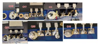
I have cleaned up my solder joints as best I can. A few are marginal. Q21 I can't clean up enough.
Lesson learned for next board. I did not notice early on that the pads between the big transistors and the 0.22 resistors are very close.
Lesson learned.
Lesson learned for next board. I did not notice early on that the pads between the big transistors and the 0.22 resistors are very close.
Lesson learned.
Attachments
There shouldn't be any continuity between the amp and the heatsink.
You should also check the output and driver transistors for shorts with your meter set on diode mode.
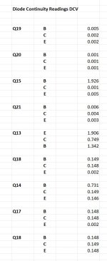
Q21 looks like a cold solder joint on the emitter and on the emitter resistors. Those two connect together anyways, so no need to worry about a short between them. You shouldn't see the solder trying to repel itself from the transistor leg. This means either the transistor was dirty, of more likely it didn't get warm enough. Same goes for the pad on the emitter resistor. Don't be afraid to get them hot. Heat until the solder flows out nicely, then remove the heat and let it cool.
You should also check the output and driver transistors for shorts with your meter set on diode mode.
Q21 looks like a cold solder joint on the emitter and on the emitter resistors. Those two connect together anyways, so no need to worry about a short between them. You shouldn't see the solder trying to repel itself from the transistor leg. This means either the transistor was dirty, of more likely it didn't get warm enough. Same goes for the pad on the emitter resistor. Don't be afraid to get them hot. Heat until the solder flows out nicely, then remove the heat and let it cool.
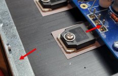
The 1 ohm reading from the screw retaining the output transisitor to the shiny metal is expected. That screw is grounded, that is why it has a shoulder washer around it. The reading from the output transistor screw to the black aluminum heatsink is also expected. The black anodizing is an insulator, usually not enough to trust for mounting transistors. That's why you use the keratherm gaskets. The readings from each rail to the shiny heatsink are both bad. You either have output transistors shorted or you have a ground connection between the transistor and heatsink because the keratherm gasket is damaged.In checking for shorts I measured as shown in the photo. My question is that the 147.0 ohm stands out as bad?
Measure from each leg of every output transistor to the shiny heatsink. All those readings should be in the kilo ohm or higher range. That will also let you find which output transistors are the problem.
1 resolder across the transistors.There shouldn't be any continuity between the amp and the heatsink.
You should also check the output and driver transistors for shorts with your meter set on diode mode.
Q21 looks like a cold solder joint on the emitter and on the emitter resistors. Those two connect together anyways, so no need to worry about a short between them. You shouldn't see the solder trying to repel itself from the transistor leg. This means the transistor was dirty, of more likely it didn't get warm enough. Same goes for the pad on the emitter resistor. Don't be afraid to get them hot. Heat until the solder flows out nicely, then remove the heat and let it cool.
Then I did the diode readings, see below.
Patchwork quilt of issues it seems.
Attachments
Yes for sure, shorted, yes.You can find shorted outputs
at these pointsWhere are you placing the leads when you took these readings?
Attachments
Your measurements are showing that there are very bad shorts between your output transistors and the heatsinks. All there measurements should read open circuit. You should remove the amp from the heat sink and check out the thermal pads. Once the amp is remove you need to re-test the output transistors.
Normally when an output transistor fails due to being overloaded it will short out internally, so the usual quick check with them in circuit is to set your meter on diode check and measure between the base and emitter, then base to collector, then collector to emitter. all these measurements should read above .6V. If there are any reading 0V there is a shorted output device in which case the set needs to be replaced and the drivers need to be tested.
As I said this is just a quick check, output devices don't always short when they fail. At this point we're just trying to determine where the amplifier is shorted, blowing the fuses.
I removed the board from the heat sink and retested using B to C and C to E. All ringing and nothing measured above .6V.
Time to move to a fresh board. I have learned a great deal thanks to all the help everyone has provided.
I'm going heads down to carefully assemble, test and install all the components, using the latest BOM provided by Stuartmp in #5215.
Time to move to a fresh board. I have learned a great deal thanks to all the help everyone has provided.
I'm going heads down to carefully assemble, test and install all the components, using the latest BOM provided by Stuartmp in #5215.
@Chiptech starting fresh at this point is probably a good idea.
Take your time.
Measure and confirm each component before you install it.
Clean your board thoroughly before you apply power.
Use a magnifier light to check that you don't have any solder bridges between pads.
Use a regulated supply for your initial start up.
You can also verify the board without the output transistors installed if you like.
This allows you to use a 50mA limit on your regulated supply so there is little chance of component damage even if something is wrong.
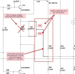
Just follow my image attachment.
Once you verify the board you can install the outputs.
Take your time.
Measure and confirm each component before you install it.
Clean your board thoroughly before you apply power.
Use a magnifier light to check that you don't have any solder bridges between pads.
Use a regulated supply for your initial start up.
You can also verify the board without the output transistors installed if you like.
This allows you to use a 50mA limit on your regulated supply so there is little chance of component damage even if something is wrong.
Just follow my image attachment.
Once you verify the board you can install the outputs.
Attachments
Last edited:
Stuartmp,
That is the plan. I believe a friend has a regulated supply I could borrow.
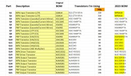
As I review all my parts, below is the list of transistors I'm using [they are on the current board]. I compared it with the latest BOM [2.5.4] but don't see any major differences, unless I'm missing something. The HFE ratings are from my actual transistor measures.
That is the plan. I believe a friend has a regulated supply I could borrow.
As I review all my parts, below is the list of transistors I'm using [they are on the current board]. I compared it with the latest BOM [2.5.4] but don't see any major differences, unless I'm missing something. The HFE ratings are from my actual transistor measures.
Attachments
this chart is incorrect R30 should show 500R value.I have reviewed the latest BOM and note the following changes:
Confirming that Trim pot R30 goes from 300R to 200R?
I can update my board after a few parts come in.
Try and match on the VBE value first then try and match the HFE value between NPN and PNP.s there an optimum Hfe target for Q14 & Q15? I just tested a lot of each and I'm averaging:
Regarding R30 using a higher value like 500R will ensure the output transistors are completely switched off during your initial start up.

As part of my 2nd effort to build the amp board I'm reviewing all the parts.
For C6 [220nF - 50V cap] is the spec, but the original BOM calls for
For C6 [220nF - 50V cap] is the spec, but the original BOM calls for
| 495-2436-ND [B32521C1224K000] which is 100V. 220nF 50V cap is hard to find. Can I use B32521C1224K000 or alternate rated @100V for C6 |
- Home
- Amplifiers
- Solid State
- diyAB Amp The "Honey Badger" build thread