Hi matt,
Thank you for the good info. However, a problem we often have here is we are usually modding boards that already have a lot of SMD parts soldered down, and we don't want to un-solder them. My own dac board has parts soldered to both sides of the ground plane, top and bottom. Also, some of my SMD work involves soldering to things other than PCB pads. I would agree in cases where there is a bare PCB to solder SMD parts to, it might be a very good choice just to cook it using a device made for that purpose or perhaps using some improvised method.
Thank you for the good info. However, a problem we often have here is we are usually modding boards that already have a lot of SMD parts soldered down, and we don't want to un-solder them. My own dac board has parts soldered to both sides of the ground plane, top and bottom. Also, some of my SMD work involves soldering to things other than PCB pads. I would agree in cases where there is a bare PCB to solder SMD parts to, it might be a very good choice just to cook it using a device made for that purpose or perhaps using some improvised method.
@pentajazz,
Unfortunately, it looks like more junk. They say it has an external linear power supply, but it is a uni-polar 5v, 2A supply only. How do the opamps work on that? Not all that well probably, or maybe there is a switcher inside for the analog stuff. Not much good the linear supply would do in that case.
Unfortunately, it looks like more junk. They say it has an external linear power supply, but it is a uni-polar 5v, 2A supply only. How do the opamps work on that? Not all that well probably, or maybe there is a switcher inside for the analog stuff. Not much good the linear supply would do in that case.
and another one here. Still looks like voltage mode, but onboard psu seems better with dual regs and seperate regs for mikro controler. AVCC psu is not so clear..
ES9038Q2M I2S DSD256 DAC HiFi Optical Coaxial Audio Decoder Assembled Board 384K | eBay
ES9038Q2M I2S DSD256 DAC HiFi Optical Coaxial Audio Decoder Assembled Board 384K | eBay
This appears to be a good board to mod. Here's what I see.
1, AVCCL and AVCCR are both fed by a couple vias from under the board. C10, C11 This should be easy to tap and separate from below. Solder the wires for AVCC from an external AVCC dual op amp supply directly to the vias by a couple pins.
2. Rip out the complete IV section on the board.
3. Even remove the Vref networks on the original board.
4. Now build a daughter board that fits directly above the empty space now vacated. On this board, you will use 4 dual op amps and build a proper IV section using one of the four.
5. There's enough space there to hold 4 dual op amps on top. Possibly have the direct output of the AVCC supply directly above the vias I mentioned above.
6. The daughter board can lay pretty much lay directly above the vacated space for short leads. I'd even consider using op amp pins as leads
Yeah, this board certainly has potential if someone really wants to polish it. Much nicer board than the one at the start of this thread and really if someone builds it up should start a new thread.
Don't know if a new thread would be a good idea, but maybe. It would still be an ES9038Q2M board type of thread, and it would for the most part still need the same functionality of mods as for the original boards. There would probably be much more commonality rather than differences. The difference might mostly be in the layout of the output stage and AVCC board (assuming there is one board for both functions).
Also, so we are using the same terms, I/V means voltage to current and we would need one dual opamp per dac channel for that, so 2 dual I/V opamps on the daughterboard, and one differential summing/filter dual opamp.
The main reason for starting a new thread might be to create a much more focused how-to modding tutorial without any other old baggage (since we now know a lot more about a formula for set of mods that works pretty well). In that case, perhaps both style boards could be included, unless maybe we decide the new board is so much better that the old board should be abandoned. However, the new board doesn't seem to have display and remote control capability available as of yet, so abandonment of the old board might be premature.
Maybe best to just wait until one gets here to study close up and in person, then maybe the best plan of action going forward will become more self-evident.
logged in to see progress and find focus has shifted to 4 more new 9038 boards....
Attention span of a geriatric goldfish round here.....lol !....ohhh...bright and shiny !!!
Oh well... that's me banned....... so long and.....
Attention span of a geriatric goldfish round here.....lol !....ohhh...bright and shiny !!!
Oh well... that's me banned....
... so long and.....Curiously enough, the dolphins had long known of the impending demolition of Earth and had made many attempts to alert mankind to the danger. But most of their communications were misinterpreted as amusing attempts to punch footballs, or whistle for titbits, so they eventually gave up and left the Earth by their own means - shortly before the Vogons arrived. The last ever dolphin message was misinterpreted as a surprisingly sophisticated attempt to do a double backwards somersault through a hoop, whilst whistling the ‘Star-Spangled Banner’. But, in fact, the message was this “So long and thanks for all the fish”.
There has not been any particular shift in focus to new boards. We do tend to take note when new ones come out and generally find out they are no better than the old one. Looks like one new one this time may be worth taking a closer look at, that's all.
Parts should be coming in later this week for me to start a tutorial on building a through-hole output stage board (for people who don't like SMD soldering). Hopefully will turn out to be interesting, easy to do, and perform well.
Katana 1.2 boards are expected to ship out to reviewers sometime this week. Hoping that happens as scheduled.
Updates:
Remaining parts for through-hole output stage and AVCC expected this Friday. Guess I know what I will be doing this weekend.
Can't wait to start the mods!
I hope iyou will provide really step by step tutorial that I can understand
Thank you Mark
Who try to replace the output capacitors and by what ?
They probably shouldn't be needed, but if you want them you could use fairly large value back to back electrolytics. Nothing else has enough capacitance not to roll off too much bass unless perhaps you know in advance that the load will have a fairly high input impedance.
Nobody to design a PCB for the Marwk4 output stage ?
If using a PCB, I would still vote for people trying to learn how to solder larger sized SMD parts. It really isn't hard so much as it may be scary looking and something new to learn. How about just get a cheap SMD practice kit, watch a one or two youtube videos and give it a go? You will be happy you did. Then an output stage PCB could be much smaller, maybe small enough to fit into one of the cases that are made for the dac boards.
That supposed to intentionally enigmatic?
Late at night, EST
The finding from that exercise is stellar for the person who wants to engineer an existing circuit or even design one from the start.
First rail voltages do matter. The discussion of the stages of the IV stages have tended to center on filtering aspects. This of course is not their primary purpose but as the name of the stage suggest, it is a current to voltage converter.
I can see that few readers have actually gone through the exercise of reading and understanding the design process.
The first thing is that it is explained how the noise figure is arrived at.
The second thing is that it exposed to me a bigger thing that there is a source resistance model to the current source.
The gist is that the first transimpedance stage follows a simple idea. Current from the dacL and dacR times the feedback resistance = the output voltage of the first stage. ( the ones with the dual op amps..transimpedance) We all know that V=IR.
For the DAC we are working with, we don't know the output current specs, well at least I do not have the equipment to measure the peak anyways. Looking at the AVCC required currents I have never seen whether the spec refers to peak. I will guess that the model that TI used was meant to be used in a potentially portable machine judging by the rail voltage limitations they placed on the design. They indicate a bit under 2 ma. Now looking at the circuit ESS provided in the near 10 year old document that is being used as a reference, we see that they suggested a value of 2.7K versus the one that TI circuit indicates should be around 2.3K for their given design. Then I checked the feedback resistor on my Ebay Dac and it is about .68K about one quarter of what the ESS circuit uses.
So for months I was asking myself why the huge difference. Good thing I learnt how this value is selected.
Remember V=IR. The I is fixed by DAC output and the V is what is at the output of the first transimpedance stage. V is also a function of the rail voltages and can make a difference depending on how high you want V to go. So R controls all of this. How high do you want V to go? as high as you can get it to maintain or minimize noise in this three op amp circuit......without overloading the input of the second stage which is the difference amplifier and /or clipping the transimpedance output stage due to rail voltage limitations.
Now what was surprising to me is that the first stage is always driven hard to high voltages. In normal filter and line gain stages, I always had a view that a semi decent high enough rail voltage hardly made any difference and indeed it is like that BUT these stages are not driven hard like the first transimpedance stage. I remember looking at the discussing between Mark and Abraxalito and the discussion of why the op amp loading could be an issue and the loading and on the surface I tended to tell myself, yeah, the dac only ouputs maybe a couple volts or so, why worry about the loading. Now I know why worry about the loading. The level it is driven at, you have no choice, it is not like you turn the volume control down, the peak voltages are happening everytime the recording engineer VU meter or peak meter swings right hard. It is in the recording itself.
So going back. If you use a DAC with a high output current, and a low rail voltage, you can easily drive the OP AMP into overload at the transimpedance stage if you choose a resistor too high. If you choose a resistor too low, then you are not optimizing the circuit. There is a balance here between rail voltage, voltage noise of the op amp and thermal noise from the feeedback resistor.
Ideally you need to know the dac current output. NOT knowing that and modifying a given dac like an Ebay PRO Sabre model, I am going to build myself some headroom and since I will be using an OPA16xx series on my Pro build, I will be raising the rail voltages to 18Volts like the DAC3. In my case it is not to mimic them but to build a cushion to ensure that my first transimpedance stage never clips on the output. I'm an ME, I like safety margins.
This expercise also shed light why Sergelisses and myself preferred the sound of the OPA16XX series because I think in the PRO Sabre series it might actually better address some other design aspects but I am thinking or analyzing that through and reading other papers to sort that out.
Also for the PRO Sabre series, the LME49600 combined with an LME49710 or AD797 ( seen that combo before....the headphone amp Mark recommends....) might be a good fast OP AMP AVCC. In fact I asked about that once and it was dismissed but when I perused the LME49600 datasheet carefully, there right in front of my eyes was the mention of a high speed power regulator. The reason these might not be used commercially is the cost. It is much cheaper to slap in a monolithic LDO regulator.
This might also explain why some people found that adding series resistance to the DAC output lowered distortion. Were they overdriving the input stage or were they overdriving the output stage of the op amp?
Listen I am just a little hobbyist not and have never taken any formal electronics courses but just scoured data sheets and read to learn and understand.
I'll discuss other things I also gleaned by reading that document and basically following how an EE proceeds with a design. Hence why I had recommended that pdf as indispensable.
I post it again as it is great as a tutorial to better understand what is happening from a simple design exercise. Even if you only know V=IR, the exercise will still make sense. Take the time to read through it.
http://www.ti.com/lit/ug/tidu672c/tidu672c.pdf
Last edited:
I hope iyou will provide really step by step tutorial that I can understand
Thank you Mark
You are very welcome, of course!
I will try to make the tutorial as clear and easy to understand as possible. What I am wondering about is about how to best layout the circuitry. Usually, if using leaded parts, I don't necessarily put them through any holes in the board unless they are big parts. Usually I just use small leaded parts and solder the leads directly to opamp socket pins on the underside of the board. Hopefully people can manage doing that okay. Not much different from soldering resistors and capacitors to tube sockets in the old days. Only difference is opamp sockets are smaller than tube sockets, and the components we use at low voltages are usually smaller too.
Thought I would mention that I sometimes use small gauge stranded wire with teflon or similar insulation as signal carrying wires. I use 28-30 or maybe even 32 gauge so it can fit between socket pins, and use insulation that is heat resistant enough to not be damaged by contact with hot solder or a soldering iron. It can be nice to have a little assortment of hookup wire including things like that.
For power wiring I usually try to use a heavier gauge wire so as to keep resistance as low as reasonably possible going back to any local bigger filter caps and all the rest of the power supply.
Sometimes I may run power on the top of the board and signals on the bottom. Will talk more about such things when we get to the actual tutorial. One of the things I am hoping is that the tutorial will cover how to plan and develop your own layouts so that in the future you may be in a better position to do your own.
@Mikett,
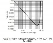
Looks like this might be a good time to try to explain something TI didn't tell you about in that app note. Attached below is a graph from the LME49720 data sheet.
What the TI guys noticed is that it shows minimum distortion using the highest possible VCC and the highest possible signal swing. (there is a different graph for each VCC, but higher is better for these graphs.)
What does the graph show and what does it mean for I/V design? Well, at the right we see that as the signal is increased distortion keeps getting lower until it rapidly starts getting higher. Why? Because they test it with a sine wave, not music. A test sine wave is at a fixed amplitude so it can be adjusted to sit and the minimum distortion point. Makes app note distortion numbers look very impressive, but it is not accurate for the distortion you will get with music, since music is not all at one fixed level. In fact, almost all of music is at a lower level where distortion is higher.
Also, distortion is going up and down all the time as music signals go through zero crossing and increase to some peak and then go down through zero to a negative peak. Happens every cycle of a tone, and every cycle of even a fixed sine wave. The distortion is dynamic and always changing.
Over at the left side of the graph we see that distortion is very high when signals are very small, as happens all the time as tones and frequencies pass through zero.
So why is the distortion so high for small signals? I will say it is because when you run an opamp on a bipolar supply, the left side of the graph shows what happens when the opamp output is going through the cross-over region.
How about if we could avoid that cross over region altogether?
The reason distortion changes with signal level is because the higher the signal level is, the less time the signal spends with the opamp output in the cross-over region. If and when we avoid that, we avoid the main source of distortion.
Okay then, the way to get minimum distortion for all levels of signals found in music is to never allow cross-over to occur. We could bias the opamp to avoid it by running in class A, but then the output would be offset, and we would need caps in the signal path which might sound even worse than the cross-over distortion.
Ah! But with an I/V stage we are already offsetting the opamps to AVCC/2 so we have an opportunity to run the opamp outputs in class A all the time and always have minimum distortion for our music signal.
What we need to do is to choose the feedback resistor so the opamp never goes closer than a few hundred millivolts from ground. That means we will get minimum distortion in this stage if we select the resistor for about a 3v or a little less peak to peak swing, and so that's what we do.
Now, let's get back to the TI app note. Suppose we are TI application engineers that have been asked by marketing to help sell more opamps. If we look at the graphs in the opamp data sheet we see that we should use maximum VCC and maximum signal levels. So we build a test circuit and using a fixed sine wave test signal we verify the distortion is really low using a signal that is right where we expected. Of course we did not try signals down at 3v swing with real dac AVCC/2 offset and all that, because we don't need to in order to write up the app note. All that stuff we can just model and sim. Unfortunately, it provides the wrong answers if designing for music!
Attachments
Last edited:
Oh, while I am still in the first transimpedance stage. If you are a keener, you will want to look carefully at specs of different op amps and study the aspects of how the output voltage and THD varies as it approaches the rail voltages. Some retain their linerarity better than others as the output voltages approaches the rail voltages and are more linear "up there". In the past, this was of hardly any consequence because most op amps in audio are not driven anywhere near the rail voltages. However in transimpedance stages in DACs, it is an engineering choice of how high you want to go. Some op amps though speced better for lower line voltages appear not to be as good for transimpedance stages when they are driven hard. Again look carefully at the specs and bahavior and choose accordingly for your application.
Look at the noise model. Running that low a voltage will degrade what you will want to do.
If I look at other similar op amps, the behaviors all follow that pattern.
I'll stick with with the design guys at TI who as best I can glean sell both the LME as well as the OPA series. So would they be fooling both the same customers.
The designer of the OPA1622 was in some forum and I also read what he had to say and that is when I took the time to look and try to understand. He seemed to be a genuinely serious audio guy and yet a sober engineer.
The ESS circuit and as best I have gleaned all have essentially the same IV circuit including the chinese ebay pro sabre dac boards. Layout is a different issue. It would be good to take the cover off the DAC 3 and see if we can identify similar IV circuitry inside and see what values they are running. You are capable of that since you've got a DAC3.
Last edited:
If you look at the I/V stage ESS designed into the ES9038PRO evaluation board, it is for about a 3v peak to peak swing. Why? Because if you look at distortion at the differential summing output with a variety of test signals and including for IMD, the distortion is lower that way. If you need really low noise too, you use all 8 output channels in parallel which reduces noise by 3dB with each doubling. Most likely, I would expect when TP releases it's 8-channel output stage for 9038PRO that will be an option.
And, no, I am not taking apart DAC-3 to suit you. Anyway, it has a mulitlayer board and tracing out circuitry in that case can be very difficult.
Maybe consider this: Why are decaying cymbal sounds so revealing of the sound of electronics? Because they are mostly very low level, almost entirely down where distortion is in fact audible.
Also, running that low a voltage will *not* degrade what I want to do. Music is at a low level during parts of every cycle, and during quiet passages. What I want is class A if I can get it.
Last edited:
If you look at the I/V stage ESS designed into the ES9038PRO evaluation board, it is for about a 3v peak to peak swing. Why? Because if you look at distortion at the differential summing output with a variety of test signals and including for IMD, the distortion is lower that way. If you need really low noise too, you use all 8 output channels in parallel which reduces noise by 3dB with each doubling. Most likely, I would expect when TP releases it's 8-channel output stage for 9038PRO that will be an option.
And, no, I am not taking apart DAC-3 to suit you. Anyway, it has a mulitlayer board and tracing out circuitry in the case can be very difficult.
Maybe consider this: Why are decaying cymbal sounds so revealing of the sound of electronics? Because they are mostly very low level, almost entirely down where distortion is in fact audible.
Also, running that low a voltage will *not* degrade what I want to do. Music is at a low level during parts of every cycle, and during quiet passages. What I want is class A if I can get it.
As I suggested in another note, take a look at the Sparkos discrete opamps. They are inherently class A and have two pole compensation. Expensive, yes, but if you are looking for the ultimate in what can be achieved, they are worthy of consideration. He also has "pro" versions which are even better, but larger form factor.
Cheers
Whit
PS - I have no fiduciary interest in Sparkos Labs, just a fan.
- Home
- Source & Line
- Digital Line Level
- ES9038Q2M Board