1. Try a ~100uF across R29, ie between output bases.
2. Short output "base blockers".
3. Remove R17 and short C5. I don't like fancy compensation because in the real world, things are not exactly as expected so keep it simple and ample. Slew rate is nice but not if it causes oscillations. And, I know D Self likes Darlington VAs but it pushes the loop gain too high where stability is difficult and/or unreliable.
4. I don't like the rail filters because to wastes output power potential and heat. If you want to do this then you need extra driver voltage, ie VCC +5V and VDD -5V, or, just use series chokes that don't drop much voltage.
Last edited:
5. A resistor in the collector of Q3 may help by separating the Q3 Ccb from the signal path.
6. Driver base capacitors sometimes work better than, or compliment the VA miller cap. Up to 1nf.
7. C18 + R42 should only be necessary for quasi-complimentary or other collector facing outputs.
8. There is no current protection, which is dangerous if you don't want to spend your life rebuilding this amp.
Last edited:
I agree with steveu's comments, but advise a little caution. A capacitor between the output bases is usually essential for high speed OP transistors, but charges up on both halves of the output swing, so could change the bias current dynamically. I would limit the capacitor to 1uF initially, and only use a larger one if accompanied with a much lower inter-base resistor (which increases the driver dissipation).
His comment #3 is the same reason I suggest using a higher emitter resistor - to reduce the OLG but more importantly, reduce the phase delays a little.
I would keep the RC load network in the output otherwise an unloaded amp's OLG may cause stability problems- at least until you track down the solution and then you could try that.
On probably a different matter, you say you have the drivers on a separate heatsink which is fine but the temperature sensing Vbe multiplier transistor should be under the control of the output transistors' die temp. for EF output stages. The drivers of EF stages are shown by Self to have fairly constant dissipation so their temperature change over the range of operation will be pretty much "do nuthin" in the usual Vbe multiplier stabilization circuit.
Ref. APADH 5th ed.
Ref. APADH 5th ed.
I would connect scope channel A to the collector of Q16 and scope channel B to the emitter of Q16 (pin 4 of connector J3). Display them both. If the emitter swings 7V past the collector, despite the presence of diode D8, that's quite a big surprise.
In fact that's Q18 (sorry for the quality of the image). I thought about that of course but I have only one osc. probe. I will have to buy another one to measure two voltages simultaneously. This is why I indicated in the attached oscilloscope images of my post #15 the position of -VCC as seen on the scope when I connect the probe to the collector of Q18.
double check your x10 scope probe compensation?
Thank you! Yes, the probe was badly overcompensated. Oh, that was why it seemed like the output voltage excursed outside the VCC rails. I borrowed the oscilloscope from a friend and just didn't think about compensation.
So one "problem" with the amp is solved!!!
I suggest using a higher emitter resistor - to reduce the OLG but more importantly, reduce the phase delays a little.
This advice is worth trying.
")
Lets think: why it only oscillates at power peaks???
(why you have positive feedback with gain > or equal than 1 only at power peaks?)
Good luck.
M.
So the oscillation problem is largely solved!
Increasing the VAS emitter resistor from 2R2 to 20R is effective indeed, it reduced the oscillation, but what was even more effective is a 680pF capacitor from VAS collector to GND. These two things together almost completely eliminated oscillation even with capacitive loads (6R parallel 100nF).
Using lower than 680pF has less effect in reducing the oscillation, any higher capacitance doesn't make it better, so 680p seems to be the best.
Unfortunately this 680pF capacitor slows down the positive slew rate to about 9V/us. The maximum slew rate of a 20kHz 40V peak voltage sine wave (that is 200W/4Ohms or 100W/8Ohm) is 5V/us, so 9V/us seems to be still acceptable, but I'm inclined to use only 470pF that allows about 13V/us positive slew rate. (thinking about high resolution audio that may contain frequencies above 20kHz).
Thank you all who tried to help!
Reducing resistors in your current mirror wil improve lover range for your darlington in vas stage. The orginal values 150 Ohm, You seems too use 450. In the range 50-100 Ohm would bee my choice of range. high values may affect one side of output halves as you affect minimum colector emitter voltage for mirror out transistor.....
So the oscillation problem is largely solved!
Increasing the VAS emitter resistor from 2R2 to 20R is effective indeed, it reduced the oscillation, but what was even more effective is a 680pF capacitor from VAS collector to GND. These two things together almost completely eliminated oscillation even with capacitive loads (6R parallel 100nF).
Using lower than 680pF has less effect in reducing the oscillation, any higher capacitance doesn't make it better, so 680p seems to be the best.
Unfortunately this 680pF capacitor slows down the positive slew rate to about 9V/us. The maximum slew rate of a 20kHz 40V peak voltage sine wave (that is 200W/4Ohms or 100W/8Ohm) is 5V/us, so 9V/us seems to be still acceptable, but I'm inclined to use only 470pF that allows about 13V/us positive slew rate. (thinking about high resolution audio that may contain frequencies above 20kHz).
Thank you all who tried to help!
Congratulations.
No better feeling than a stable circuit!
But, can you elaborate about the possible mechanism of your oscillation?
You know there are tons of Lin/Blameless builders out there that can benefit from your experience.
Thanks very much and enjoy.
M.
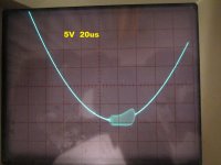
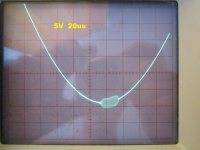
I'm back again, because my "almost completely eliminated oscillation" sentence was an overstatement. It indeed dropped to about 1/13 of its original amplitude. But that amplitude was about 40V p-p. With 470pF capacitor from VAS collector to GND, and a 20R VAS emitter resistor the oscillation is still about 3V p-p. And I'm afraid it can radiate RF via the speaker cable. The oscillation starts when the output voltage comes closer than about 2V to the negative clipping voltage. See images! I plan to post images with the Baker clamp removed tomorrow. It's a bit different without the Baker clamp - it doesn't oscillate anymore once the bottom (flat) portion of the curve is reached, but comes out of clipping (hard saturation) quite abruptly.
I used FDH400 for the Baker clamp (very similar to BAV21). It seems that whether the Baker clamp is in place or not, phase inversion or significant phase shift of the VAS occurs near clipping, so the feedback becomes positive and >1. The oscillation frequency is around 1.1MHz. The amp is solid even with capacitive loads if not driven near to negative clipping. The problem is always the negative clipping.
I used FDH400 for the Baker clamp (very similar to BAV21). It seems that whether the Baker clamp is in place or not, phase inversion or significant phase shift of the VAS occurs near clipping, so the feedback becomes positive and >1. The oscillation frequency is around 1.1MHz. The amp is solid even with capacitive loads if not driven near to negative clipping. The problem is always the negative clipping.
Attachments
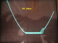
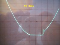
So here are the images with the Baker clamp removed. It seems the Baker clamp only helps the amp in coming out of saturation, it actually worsens the oscillation.
No wonder: When the Baker clamp acts, it bypasses the VA transistor so the inverting action of the VAS is diminished becoming a non-inverting stage and the overall feedback may actually become positive. Even makes me think... that the the higher the phase margin is (the more stable the amp), the more disastrous the feedback may become if the VAS goes non-inverting from inverting...
LTSpice showed some tendency to oscillation when coming out of clipping but it also showed that the Baker clamp does away with it. Well, not in reality. I think the problem is that as soon as the voltage peak gets near clipping and the signal gets too distorted, the input stage current mirror "bottoms out" and drives the VAS "too hard", so to say in laymen's terms.
I'm neither a fan of high loop gain at low frequencies, nor against it, the high loop gain of this circuit comes as a byproduct of the current mirror (to linearize the IPS) and the beta enhancer (to linearize the VA transistor). If I remove the current mirror, then the IPS will be the main source of overall distortion and if I remove the beta enhancer then the VA transistor will be the main source of distortion.
And I don't want to increase the Miller cap (Cdom), because the amp is rock solid even into very capacitive loads, so the thing is not about overall loop instability.
Wonder if there is any means to clamp the input stage near clipping, because I feel the problem is best handled just there.
Also tried a few changes with the OPS, but it said: "Thanks, I'm fine, I'm just doing what I'm told to do!"
Also wonder why so many people who have built the Blameless have not run into this problem.
Attachments
Last edited:
And why it oscillates only at negative clipping? I think (again in laymen's terms) the VAS has a tightly fed back current source that effectively "resists" sourcing more and more current at positive clipping. But at negative clipping nothing stops the VAS from trying to sink more and more current, except for it's emitter resistor.
Going back to the PCB you posted a while back, I see you have a great big trace loop in series with C5. Years ago I had a problem like this and I had to put the miller cap on the bottom of the board because the VA transistor was an RF oscillator using the miller cap and the PCB trace inductance. You may also want to reduce R13 to about 470 Ohms and/or bypass the collector of Q7 to the negative rail (C4,C6) with about 100n. This will move the Q7 pole up away from the dominant pole and maybe then 47P will be enough. But 47p is really pushing it. A stable amp normally uses at least 100p.
A month ago I had exactly the same problem with my Amnesis amp. After much frustration I remembered Dr Leach and DestroyerX recommended in some instances to put the zobel AFTER the output RL.
I did it. I removed the RC and soldered it at the speaker binding posts for convenience. That completelly stoped oscillations and I was able to enjoy the amp since.
I have 10R as output and 15R+100nf to ground.
I suspect the Zobel was introducing HF oscillations into ground that excited at peaks the input when it was on board.
I hope this helps.
M
Hi Steveu,
thank you for caring so much about my case. Hope I can reciprocate it some way in the future, if it might be possible.
My solution of loading down the VA collector by 470pF is really crude, makes the positive slew rate very poor, and doesn't cure the oscillation completely, so I don't really like it.
To tell the truth I was also worried about the long traces around the compansation caps, so I incorporated some inductances at these connections in the LTSpice simulation, but no oscillation effect was visible in simulation except if I entered unrealistic inductance values (>600nH that correspond to >60cm [=2 feet] long traces). I think the Miller cap of 47nF is too small to cause a resonance around 1MHz (where it actually occurs) with realistic PCB trace inductances. And the loop area? there is a solid GND plane above it, so hopefully it's not doing any harm. But since it cured you amp, I'm gonna try to reduce the trace lengths if nothing else works...
The ULGF is dependent not only on the Miller cap value but also for example on the LTP degeneration resisitors (actually on 1/gm+degen. R) a higher degen R needs a lower Miller C (for the same unity loop gain crossover freq.). The original Blameless design used 100R, mine is 150R. Actually I always look at the ULGF which is around 0.9MHz with 47pF (shown by simulation) doesn't seem too high with the fast transistors I use. If I recall DIYaudio member dadod used the same VA, driver and output transistors with ULGF around 2MHz in his designs. Now I would deem 2MHz can be REALLY pushing the limits and you may find yourself at the mercy of component tolerances. Well, I may be forced to take the Cdom higher, but I still hope there may be some other problem here waiting to be found.
About the highish value of R13: Usually 1k is used in that place as the collector resistor for the beta-enhancer, and that allows the beta-enhancer to inject about 40mA into the VA base during negative clipping if the Baker clamp diode or clamp transistor is not there (and assuming 50V HT rails). (The Baker clamp was a later addition to my circuit, still a bit hesitant to use it or not...) So I said why not use 5.6k for R13 that limits this base current to about 7mA. With 5.6k no degradation effect was seen in simulation, but you may be right it wasn't a good idea. I have not the faintest idea how much max. base current the KSC3503 should be able to take, the datasheet is silent, it only lists max. collector current at 100mA. There are BJT's that can take max. 1/5 of the max. collector current at the base (like KSC1845-KSA992 for example). The KSC3503 might be able to take even the 80mA base current during negative clipping which results from the 470R you suggest. Or it may be damaged after a while. Who knows? Of course if the baker clamp is in place, then it doesn't matter.
Yes, the 100nF bypass to negative rail is definitely something I want to try!!!
thank you for caring so much about my case. Hope I can reciprocate it some way in the future, if it might be possible.
My solution of loading down the VA collector by 470pF is really crude, makes the positive slew rate very poor, and doesn't cure the oscillation completely, so I don't really like it.
Going back to the PCB you posted a while back, I see you have a great big trace loop in series with C5. Years ago I had a problem like this and I had to put the miller cap on the bottom of the board because the VA transistor was an RF oscillator using the miller cap and the PCB trace inductance.
To tell the truth I was also worried about the long traces around the compansation caps, so I incorporated some inductances at these connections in the LTSpice simulation, but no oscillation effect was visible in simulation except if I entered unrealistic inductance values (>600nH that correspond to >60cm [=2 feet] long traces). I think the Miller cap of 47nF is too small to cause a resonance around 1MHz (where it actually occurs) with realistic PCB trace inductances. And the loop area? there is a solid GND plane above it, so hopefully it's not doing any harm. But since it cured you amp, I'm gonna try to reduce the trace lengths if nothing else works...
You may also want to reduce R13 to about 470 Ohms and/or bypass the collector of Q7 to the negative rail (C4,C6) with about 100n. This will move the Q7 pole up away from the dominant pole and maybe then 47P will be enough. But 47p is really pushing it. A stable amp normally uses at least 100p.
The ULGF is dependent not only on the Miller cap value but also for example on the LTP degeneration resisitors (actually on 1/gm+degen. R) a higher degen R needs a lower Miller C (for the same unity loop gain crossover freq.). The original Blameless design used 100R, mine is 150R. Actually I always look at the ULGF which is around 0.9MHz with 47pF (shown by simulation) doesn't seem too high with the fast transistors I use. If I recall DIYaudio member dadod used the same VA, driver and output transistors with ULGF around 2MHz in his designs. Now I would deem 2MHz can be REALLY pushing the limits and you may find yourself at the mercy of component tolerances. Well, I may be forced to take the Cdom higher, but I still hope there may be some other problem here waiting to be found.
About the highish value of R13: Usually 1k is used in that place as the collector resistor for the beta-enhancer, and that allows the beta-enhancer to inject about 40mA into the VA base during negative clipping if the Baker clamp diode or clamp transistor is not there (and assuming 50V HT rails). (The Baker clamp was a later addition to my circuit, still a bit hesitant to use it or not...) So I said why not use 5.6k for R13 that limits this base current to about 7mA. With 5.6k no degradation effect was seen in simulation, but you may be right it wasn't a good idea. I have not the faintest idea how much max. base current the KSC3503 should be able to take, the datasheet is silent, it only lists max. collector current at 100mA. There are BJT's that can take max. 1/5 of the max. collector current at the base (like KSC1845-KSA992 for example). The KSC3503 might be able to take even the 80mA base current during negative clipping which results from the 470R you suggest. Or it may be damaged after a while. Who knows? Of course if the baker clamp is in place, then it doesn't matter.
Yes, the 100nF bypass to negative rail is definitely something I want to try!!!
The ULGF is dependent not only on the Miller cap value but also for example on the LTP degeneration resisitors (actually on 1/gm+Rdegen) a higher Rdegen needs a lower Miller C (for the same unity loop gain crossover freq.). The original Blameless design used 100R, mine is 150R. Actually I always look at the ULGF which is around 0.9MHz with 47pF (shown by simulation) 0.9MHz doesn't seem too high with the fast transistors I use.
Necessary Cdom also depends inversely on the closed loop gain Acl, which is higher in my amp than in the original Blameless. So I think we can rest assured 47pF in my design is not very low.
The KSC3503 might be able to take even the 80mA base current during negative clipping which results from the 470R you suggest.
But alas! KSC1845 (Q7) can only carry a max. 50mA collector current, so the 1k resistor for R13 is definitely the minimum safe value without the baker clamp in place. Anyway, according to simulation the small ringing present with 5.6k only gets worse with lower values like 1k or 470R...
I also checked the workings of a 100nF capacitor from Q9 (KSC3503) collector to the filtered negative supply in simulation, without baker clamp. Unfortunately this cap forces Q7 output currents in excess of 200mA into the base of Q9 even if for only a few tens of microsecs at the beginning of negative clipping. Wonder if KSC1845 and KSC3503 can take it on the long run. It's outside their abs. max. ratings. With this cap, simulation also showed a nasty glitch of output voltage on entering negative clipping.
Still worth trying perhaps...
- Status
- This old topic is closed. If you want to reopen this topic, contact a moderator using the "Report Post" button.
- Home
- Amplifiers
- Solid State
- Help! Oscillation and "rail override" problem with my power amp