Just an idea - what about using a high speed BJT follower after the logic gate. An RF BJT will have from <1pF to 2pF load on the logic and it will have lower OP Z of a few ohms or less if you load it with more current.
This would be very easy to implement and the extra class A loading could be a simple resistor to a - supply.
T
This would be very easy to implement and the extra class A loading could be a simple resistor to a - supply.
T
Hi andrea_mori
I use 7400 series bus storage registers for the Mosaic UV and 7400 bus storage registers and 7400 series octal D flip-flops for the Mosaic II. These are similar devices as used in most discrete R2R ladder DACs.
We have to face the fact that there are no perfect components, ok we might get parts with say 1 Ohm RDSon but these will cause new problems (higher surge currents, higher ground-bounce, more pollution) especially with the given parasitics of a relatively large discrete circuit.
The same imperfect devices can be used in different ways to improve performance. The Mosaic converter circuit -looks- similar to conventional discrete R2R ladder DAC circuits, except, it is no R2R ladder DAC.
Most popular discrete R2R ladder DACs are based on simple voltage attenuators based on two resistors (R and 2R).
For higher precision Wheatstone bridges are used:
Wheatstone bridge - Wikipedia
That's what I used for the Mosaic matrix converter and that's why accuracy is no longer an issue.
The remaining small bit errors are below the audibility threshold. These errors can be easily nulled by trimming.
I personally would be much more concerned about the (interface) noise spectra that are unavoidable with digital audio.
just a curiosity about ternary logic switches, are you using discrete devices or logic IC (flip-flop, latch) like Soekris or Rockna's devices?
I use 7400 series bus storage registers for the Mosaic UV and 7400 bus storage registers and 7400 series octal D flip-flops for the Mosaic II. These are similar devices as used in most discrete R2R ladder DACs.
I have not yet decided which is the best way, there are advantages and disadvantages in both cases. With discrete parts you can reach very low RDS-on (20-30 mOhm or so), but they are slower that logic ICs. Also the logic to drive discrete switches is more complex and p-channel devices are tipically different from n-channel devices (RDS-on, input and output capacitance, speed).
Conversely logic ICs are simpler to drive, are faster but have greater RDS-on (10 to 20 ohm or so), that finally affects the ladder network precision (monotonicity).
We have to face the fact that there are no perfect components, ok we might get parts with say 1 Ohm RDSon but these will cause new problems (higher surge currents, higher ground-bounce, more pollution) especially with the given parasitics of a relatively large discrete circuit.
The same imperfect devices can be used in different ways to improve performance. The Mosaic converter circuit -looks- similar to conventional discrete R2R ladder DAC circuits, except, it is no R2R ladder DAC.
Most popular discrete R2R ladder DACs are based on simple voltage attenuators based on two resistors (R and 2R).
For higher precision Wheatstone bridges are used:
Wheatstone bridge - Wikipedia
That's what I used for the Mosaic matrix converter and that's why accuracy is no longer an issue.
The remaining small bit errors are below the audibility threshold. These errors can be easily nulled by trimming.
I personally would be much more concerned about the (interface) noise spectra that are unavoidable with digital audio.
Hi John!
I just wanted to point that I mentioned you, and your research, in a recent post... here:
Integral nonlinearity (INL), THD, etc., in multi-bit DACs
I just wanted to point that I mentioned you, and your research, in a recent post... here:
Integral nonlinearity (INL), THD, etc., in multi-bit DACs
For higher precision Wheatstone bridges are used:
Wheatstone bridge - Wikipedia
That's what I used for the Mosaic matrix converter and that's why accuracy is no longer an issue.
The remaining small bit errors are below the audibility threshold. These errors can be easily nulled by trimming.
Well, I have a little preference for the discrete devices.
They have some drawbacks but since they have to switch at a relatively low frequency (44 to 192 or maybe 384kHz) they are not so bad.
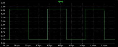
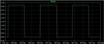
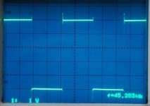
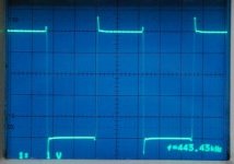
In the attached picture the simulation (48kHz and 384kHz) and the real measurement (45 kHz and 443kHz) of a mosfet pair in SO-8 package.
The waveform is beatiful at 45kHz and still looks good enough at 443kHz. The ground bounce can be decreased with a better driver circuit.
The advantage of this configuration is that they have very low output impedance, 38 mOhm for the N-channel and 66 mOhm for the P-channel, that means less than 0.001% with a 10K ladder (17-18 bit accuracy).
BTW, I can't figure out how a Weathstone bridge can help with DAC accuracy. You need anyway precise resistors to balance the bridge (or to unbalance it at certain current/voltage) unless you trim individually each bridge or you use some artifacts to get a dynamic correction of the error due to the resistances tolerance.
Moreover, let say a 74LVC574 has an output impedance around 23 Ohm when it switches low and around 25 Ohm when it switches high, at least 350 times higher than the mosfet pair. This resistance is in series with the ladder, so with a 10k ladder it weights at least 0.25%.
This resistance could be part of the bridge so it does not affect the balance, but:
- the other resistances of the bridge have to be very precise
- there is anyway a difference around 2 ohms between the low/high logic states (at least 0.01% with a 10k ladder)
What is missing?
Attachments
Last edited:
Hi andrea_mori
Slower logic in combination with parasitics causes unwanted glitches. Low RDSon in combination with parasitic capacitance and inductance causes ground bounce and ringing even before a resistor is attached.
What we need is fast logic that produces minimum ground-bounce and ringing. After testing many different logic family versions I ended up using fast logic with 8mA output current, RDSon high = 43 Ohms, RDSon low = 32 Ohms.
Best results at higher sample rates and lowest noise are obtained using lowest practical resistor values. In the Mosaic Matrix DAC I can go as low as 250 Ohm network impedance.
The Mosaic matrix converter is sensitive to resistor tolerances and RDSon high/low -mismatch- between driver circuits. However, before trimming the average bit error (80+ units tested) is already below the audibility threshold. After trimming -60, -70 and -80dB test signals look fine on the scope. Even dither patterns are clearly visible.
I used these test tracks for trimming:
Test CD
R2R ladder DACs are sensitive to resistor tolerances and absolute RDSon of the driver circuits.
There are ways to reduce RDSon related error in R2R ladder converters:
1) Calculate the average RDSon value (RDSon high + RDSon low) /2. With 43 and 32 Ohms we get 37.5 Ohm average RDSon. Subtract this value from the 2R resistor connected to the driver. For example when using 10K for 2R, we could add a high Ohmic shunt resistor so we get a new 2R value of 9962.5 Ohms.
2) Use two tri-state drivers for each bit. Enable one driver (/OE = 0) when data = 1 and the other driver (/OE = 0) when data = 0. Connect the inputs of the tri state drivers to VDD and VSS respectively. This requires an additional inverter to drive both /OE inputs.
Now connect a 10000 Ohms - 43 Ohms = 9957 Ohms resistor to the tri-state high driver and a 10000 Ohms - 32 Ohms = 9968 Ohms resistor to the tri-state low driver. Connect the other wire of both resistors together and to the ladder. Again high Ohmic shunt resistors can be used to get exact value.
This way it is also possible to compensate for RDSon low and RDSon high tolerances of each driver.
They have some drawbacks but since they have to switch at a relatively low frequency (44 to 192 or maybe 384kHz) they are not so bad.
Slower logic in combination with parasitics causes unwanted glitches. Low RDSon in combination with parasitic capacitance and inductance causes ground bounce and ringing even before a resistor is attached.
What we need is fast logic that produces minimum ground-bounce and ringing. After testing many different logic family versions I ended up using fast logic with 8mA output current, RDSon high = 43 Ohms, RDSon low = 32 Ohms.
Best results at higher sample rates and lowest noise are obtained using lowest practical resistor values. In the Mosaic Matrix DAC I can go as low as 250 Ohm network impedance.
The Mosaic matrix converter is sensitive to resistor tolerances and RDSon high/low -mismatch- between driver circuits. However, before trimming the average bit error (80+ units tested) is already below the audibility threshold. After trimming -60, -70 and -80dB test signals look fine on the scope. Even dither patterns are clearly visible.
I used these test tracks for trimming:
Test CD
R2R ladder DACs are sensitive to resistor tolerances and absolute RDSon of the driver circuits.
There are ways to reduce RDSon related error in R2R ladder converters:
1) Calculate the average RDSon value (RDSon high + RDSon low) /2. With 43 and 32 Ohms we get 37.5 Ohm average RDSon. Subtract this value from the 2R resistor connected to the driver. For example when using 10K for 2R, we could add a high Ohmic shunt resistor so we get a new 2R value of 9962.5 Ohms.
2) Use two tri-state drivers for each bit. Enable one driver (/OE = 0) when data = 1 and the other driver (/OE = 0) when data = 0. Connect the inputs of the tri state drivers to VDD and VSS respectively. This requires an additional inverter to drive both /OE inputs.
Now connect a 10000 Ohms - 43 Ohms = 9957 Ohms resistor to the tri-state high driver and a 10000 Ohms - 32 Ohms = 9968 Ohms resistor to the tri-state low driver. Connect the other wire of both resistors together and to the ladder. Again high Ohmic shunt resistors can be used to get exact value.
This way it is also possible to compensate for RDSon low and RDSon high tolerances of each driver.
Interestingly, a very scrupulous test. In what standard are the tracks made? 44,1/16?
Hi andrea_mori
Slower logic in combination with parasitics causes unwanted glitches. Low RDSon in combination with parasitic capacitance and inductance causes ground bounce and ringing even before a resistor is attached.
Hi John,
I'm not much worried about glitch, I use sign magnitude notation (so the MSB doesn't switch at every zero crossing), and also first 5 MSBs are thermometer docoded, so only a switch turns on at a time. Finally voltage output DAC helps to decrease the glitch.
Rather I'm a little worried about ground bounce and ringing, clearly visible in the plots I posted. So I'm investigating about the various flip-flop families.
Firstly I would say that a good practice should be using single flip-flop instead of multiple (octal or so on), to avoid any loop between the flip-flops. This should help to decrease the ground bounce.
Also, with single flip-flops I can install a bypass capacitor for each one, helping again to reduce the ground bounce.
There is not a great choice of single flip-flop with 3-state output: there is the NXP 74AUP family, very fast devices but very low current output (4mA at 3V) and very high RDS-On (around 100 ohms). Then there are the TinyLogic from Fairchild and the LVC family from TI, very similar, slower than the NXP but with much more output current (24mA at 3V) and lower RDS-On (23-25 ohms).
Time to do some tests.
On the accuracy side I believe that we need at least 16-17 bit. Since a RDS-On of 23-25 Ohms or more heavily affects the accuracy of the ladder network most part of the switches need fine trimming (at least first 16 MSB).
-60dB means 10 bit of accuracy, we need at least -90dB (16 bit).
In my design the first 5 MSB are not affected by the RDS-On of the active devices, because the thermometer decoder doesn't care about the resistance in series between the active device and the resistor of the ladder. Anyway I have to trim at least 11 bit, not a simple job.
The test tracks are very interesting, but why not to trim every bit in DC?
Using a 6.5 digits DMM one could switch one bit at a time measuring directly the DC voltage at the output.
Andrea
Hi andrea-Mori,
The flip-flops should drive the /OE inputs of a tri-state buffer pair. One flip-flop, two tri-state buffers. Tri-state buffer #1 drives the 2R resistor that is compensated for RDSon high and buffer #2 drives the 2R resistor that is compensated for RDSon low. The buffer inputs (A) are connected to VDD and VSS respectively and the /OE inputs are driven by the flip-flop Q and /Q outputs.
The longer the traces between flip-flops and other circuits, the higher the trace inductance the more problems.
Anyway, designing and building a good discrete D/A converter is child's play compared to the many issues introduced by data timing and noise signals.
Also keep in mind that a significant number of LSBs will be masked by (ambient) noise, especially at lower (comfortable) volume settings.
Rather I'm a little worried about ground bounce and ringing, clearly visible in the plots I posted. So I'm investigating about the various flip-flop families.
Firstly I would say that a good practice should be using single flip-flop instead of multiple (octal or so on), to avoid any loop between the flip-flops. This should help to decrease the ground bounce.
Also, with single flip-flops I can install a bypass capacitor for each one, helping again to reduce the ground bounce.
The flip-flops should drive the /OE inputs of a tri-state buffer pair. One flip-flop, two tri-state buffers. Tri-state buffer #1 drives the 2R resistor that is compensated for RDSon high and buffer #2 drives the 2R resistor that is compensated for RDSon low. The buffer inputs (A) are connected to VDD and VSS respectively and the /OE inputs are driven by the flip-flop Q and /Q outputs.
The longer the traces between flip-flops and other circuits, the higher the trace inductance the more problems.
Anyway, designing and building a good discrete D/A converter is child's play compared to the many issues introduced by data timing and noise signals.
Also keep in mind that a significant number of LSBs will be masked by (ambient) noise, especially at lower (comfortable) volume settings.
What about a TDA1541A related post for a change ")
Some weeks ago I picked up the TDA1541A project again as DIY audio members asked for this. It resulted in a rather strange design that performs exceptionally well. I plan to publish schematics for DIY.
I needed some digital audio receiver to experiment with so I used a DIR9001 receiver board I designed for the Mosaic Toslink project. I configured it for left justified so it was easier to design a discrete protocol converter that outputs simultaneous data (Data Left, Data Right, bit clock and Latch Enable).
The advantage of simultaneous data is that we can have 48 bit silence after clocking in L + R data simultaneously. This greatly reduces on-chip ground-bounce. Now the outputs can be latched with a separate latch signal (LE) when ground bounce has reached zero so on-chip trigger uncertainty will be as low as it gets.
The protocol converter inverts the MSBs on the fly, lines up L and R channel data and creates short 16 bit data and clock bursts followed by 48 bit silence.
The protocol converter uses very little power (few milli amps) and runs on 2V4 so I don't need attenuator circuits on the digital interface inputs. It produces extremely low switching noise compared to an ASIC or similar programmable logic.
TDA1541A was placed in simultaneous mode (pin 27 tied to -5V).
And then there was the DEM circuit problem again, RF interference all over the place and poor low level performance. So I decided to try low frequency DEM. I set up the DEM oscillator for approx. 50Hz (1uF between pins16 & 17, 12K between pin 15 and 17 for bias). Yes, 50 Hz as in 50Hz mains frequency.
After some experimenting I ended up installing 14 x 100uF/25V for filtering. Plus goes to GND as the DC voltage on the decoupling pins is negative. These capacitors take up to 30 seconds to charge as these have to be charged with the low bit currents. There will be heavy distortion at power up that slowly disappears as the capacitors charge and start averaging the active divider output currents.
I was worried about DC leakage current and low level performance. However low level measurements showed very good low level performance even with a plain A chip all the way down to -80dB.
This simple DEM mod can be used with every TDA1541A-based design.
Decoupling is far less critical now as the highest frequency equals only 50Hz. The ripple voltage on all pins was too low to measure with my scope. The absence of continuous RF noise also makes the power supply less critical.
For passive I/V I use 150 Ohms, without further measures this leads to heavy distortion because of the negative DC offset caused by -2mA bias (0.002 * 150 = -300mV). I added a 2K2 bias resistor between output and +5V. Now I get low distortion 600mVpp at the TDA1541A output. This signal can either drive a sensitive (pre) amp directly or one can add a pre amp circuit like the Aikido tube or semiconductor amp.
One might connect multiple TDA1541A chips in parallel in order to lower the I/V resistor value.
Now one could drive a step up transformer while maintaining reasonably low output impedance (I/V resistor value times transformation ratio squared). This enables fully passive output with low enough output impedance to directly drive a (pre) amplifier.
Some examples:
One converter, 600mVpp 150 Ohms, 1:2 step-up, 1.2Vpp out 600 Ohms output impedance. 1 x TDA1541A for stereo
Two converters (dual mono), 600mVpp, 75 Ohms, 1:3 step up, 1.8Vpp out, 675 Ohms output impedance. 2 x TDA1541A for stereo
4 converters (dual-dual mono), 600mVpp 37.5 Ohms, 1:4 step up, 2.4Vpp out, 600 Ohms output impedance. 4 x TDA1541A for stereo.
Great simultaneous project. Thanks dear Guru.
So they have to be high Q, low leakage. What about tantalum?
Now, where to find some chips from a reputed seller?
Best wishes,
M.
After some experimenting I ended up installing 14 x 100uF/25V for filtering. Plus goes to GND as the DC voltage on the decoupling pins is negative. These capacitors take up to 30 seconds to charge as these have to be charged with the low bit currents. There will be heavy distortion at power up that slowly disappears as the capacitors charge and start averaging the active divider output currents.
So they have to be high Q, low leakage. What about tantalum?
Now, where to find some chips from a reputed seller?
Best wishes,
M.
Thanks John for sharing (once again) the insight that results from your excellent work. The good performance that you have achieved motivates me to try the TDA1541A for a change, with your recommendations.
My only question is about the passive I/V to ground. Henk Ten Pierick suggested that in order to achieve a constant current draw on all regulators, the audio current should be coming entirely from the +5 regulator. Isn´t it beneficial to have a nearly constant current on all regs?
Something like this could do the trick. But now the signal ground is +5V. The Idss of the lower fet should be 2mA less than the upper fet. Or you could degenerate the CCS to adjust for 0V at the source. If using 2SK170 we should strive for operation near the zero tempco which is around 8mA iirc. Just an idea.
(Just realized that Vgs will swing slightly positive on the upper fet. Some say this is not desirable, any thoughts?)
Attachments
15VA Green Square 15W Sealed toroidal transformers M15-04 AC dual 15V(2*15V) | eBay
I have this transformer and it reads 18.8V is this normal?
I have this transformer and it reads 18.8V is this normal?
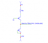
Here are the first schematics to clear things up.
U1, U2, and U3 are voltage regulators for +5V, -5V, and -15V respectively. Different types of regulators can be used here.
Very important !!, feed clean, low ripple DC voltages to these regulators.
Rectify and smoothen the voltage close to the transformer. Put some kind of pre regulator close to the smoothing cap and then run the -clean- stabilised DC voltage to the voltage regulators on the DAC module.
This minimises rectifier ripple currents being fed into the DAC module.
It is best to minimise the coupling capacitance between both primary and secondary transformer windings. Use small (few VA) transformers with dual coil former.
TDA1541A is put in simultaneous mode (pin 27 connected to -5V).
Left channel data (DOL) and Right channel data (DOR) are clocked in with BCKO. Data is latched into the TDA1541A (simultaneous mode) on the -negative- going edge of BCKO. After 16 BCKO pulses all 16 bit stereo data is loaded and BCKO, DOL, and DOR signals are shut down (zero).
MSBs must be inverted!
We wait another 16 bits and then generate a LEO pulse to latch the TDA1541A outputs. Because the interface signals BCKO, DOL and DOR were already shut down 16 bits ago -and- DEM frequency is very low, ground-bounce is very low when the outputs are latched. This translates to more accurate timing and lower on-chip jitter.
Finally we wait another 32 bits before we repeat this sample loading and latching sequence.
The DEM oscillator runs at approx. 50Hz. I use a 1uF film timing cap for this.
The 12K DEM bias resistor minimises jitter and improves stability when data is streaming. The datasheet DEM oscillator works excellent when no data is streamed but runs into -big- troubles (jitter, instability) when the data stream starts. The 12K DEM bias resistor fixes this problem.
The DEM clock is still free running as with the datasheet application.
When using multiple TDA1541A chips to lower output impedance (I/V resistor) simply copy this DEM oscillator circuit for each chip, no need for synchronising.
The 100uF/25V decoupling caps are not critical. Leakage current is no problem as extensive (low level) measurements showed. I use 100uF/25V UKA capacitors and these work just fine.
I tested -many- active I/V converters and none of these offered satisfying results. Even a plain CCS, differential stage or OP-amp causes -big- problems.
IF we had perfect active devices all conventional circuits could actually work perfectly. But when using imperfect active parts one has to go to extremes in order to get some satisfying results.
One of the problems could be thermal memory as Maxlorenz suggested. I experimented with thermal memory reduction circuits and my personal conclusion is that it is -essential- to take thermal memory effects into account when designing semiconductor based audio circuits.
Anyway I use 150R passive I/V resistor with 2K2 bias resistor to get 600mVpp low distortion output signal. One can use a suitable (tube) pre-amp to amplify this signal to the desired output voltage.
Try to keep the gain of the active circuit as low as possible, the more gain, the more distortion.
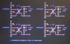
Alternative is using a -high quality- step up transformer.
The output impedance roughly equals the input impedance times the transformation ratio squared. In other words, the higher the transformation ratio, the higher the output impedance.
So if we want higher output voltage and a maintain low output impedance we need higher full-scale current (TDA1541A chip outputs in parallel) so we can lower the I/V resistor value.
The second screen shot shows some step-up transformer configurations using 1 (4mA), 2 (8mA), 4 (16mA) , or 8 (32mA) TDA1541A chips.
The amplified signal can directly drive a power amplifier.
One could also experiment with TVC that has a gain tap. This way one also has passive volume control.
U1, U2, and U3 are voltage regulators for +5V, -5V, and -15V respectively. Different types of regulators can be used here.
Very important !!, feed clean, low ripple DC voltages to these regulators.
Rectify and smoothen the voltage close to the transformer. Put some kind of pre regulator close to the smoothing cap and then run the -clean- stabilised DC voltage to the voltage regulators on the DAC module.
This minimises rectifier ripple currents being fed into the DAC module.
It is best to minimise the coupling capacitance between both primary and secondary transformer windings. Use small (few VA) transformers with dual coil former.
TDA1541A is put in simultaneous mode (pin 27 connected to -5V).
Left channel data (DOL) and Right channel data (DOR) are clocked in with BCKO. Data is latched into the TDA1541A (simultaneous mode) on the -negative- going edge of BCKO. After 16 BCKO pulses all 16 bit stereo data is loaded and BCKO, DOL, and DOR signals are shut down (zero).
MSBs must be inverted!
We wait another 16 bits and then generate a LEO pulse to latch the TDA1541A outputs. Because the interface signals BCKO, DOL and DOR were already shut down 16 bits ago -and- DEM frequency is very low, ground-bounce is very low when the outputs are latched. This translates to more accurate timing and lower on-chip jitter.
Finally we wait another 32 bits before we repeat this sample loading and latching sequence.
The DEM oscillator runs at approx. 50Hz. I use a 1uF film timing cap for this.
The 12K DEM bias resistor minimises jitter and improves stability when data is streaming. The datasheet DEM oscillator works excellent when no data is streamed but runs into -big- troubles (jitter, instability) when the data stream starts. The 12K DEM bias resistor fixes this problem.
The DEM clock is still free running as with the datasheet application.
When using multiple TDA1541A chips to lower output impedance (I/V resistor) simply copy this DEM oscillator circuit for each chip, no need for synchronising.
The 100uF/25V decoupling caps are not critical. Leakage current is no problem as extensive (low level) measurements showed. I use 100uF/25V UKA capacitors and these work just fine.
I tested -many- active I/V converters and none of these offered satisfying results. Even a plain CCS, differential stage or OP-amp causes -big- problems.
IF we had perfect active devices all conventional circuits could actually work perfectly. But when using imperfect active parts one has to go to extremes in order to get some satisfying results.
One of the problems could be thermal memory as Maxlorenz suggested. I experimented with thermal memory reduction circuits and my personal conclusion is that it is -essential- to take thermal memory effects into account when designing semiconductor based audio circuits.
Anyway I use 150R passive I/V resistor with 2K2 bias resistor to get 600mVpp low distortion output signal. One can use a suitable (tube) pre-amp to amplify this signal to the desired output voltage.
Try to keep the gain of the active circuit as low as possible, the more gain, the more distortion.
Alternative is using a -high quality- step up transformer.
The output impedance roughly equals the input impedance times the transformation ratio squared. In other words, the higher the transformation ratio, the higher the output impedance.
So if we want higher output voltage and a maintain low output impedance we need higher full-scale current (TDA1541A chip outputs in parallel) so we can lower the I/V resistor value.
The second screen shot shows some step-up transformer configurations using 1 (4mA), 2 (8mA), 4 (16mA) , or 8 (32mA) TDA1541A chips.
The amplified signal can directly drive a power amplifier.
One could also experiment with TVC that has a gain tap. This way one also has passive volume control.
Attachments
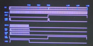
The 24bit Left Justified to Simultaneous converter.
This format can be selected on most receivers. Left justified format is easier to work with as MSB is aligned with WS. With I2S, MSB is delayed one bit with respect to WS and this translates to a more complicated circuit and more switching noise.
Attached screen shot of the timing diagram shows what we are trying to achieve.
We have DI (16 ... 24 bits). R channel is present when WSI (Word Select Input) is low. Left channel data is present when WSI is high.
MSB appears immediately after a WS change ("1" -> "0" or "0" -> "1"). I indicated this with MSB INV (MSB Invert).
MSB has to be inverted for Simultaneous mode on the TDA1541A, the other bits should not be inverted.
BCKO generates 16 pulses and then stops for the remaining 48 bits in a 64 bit frame. The TDA1541A in simultaneous mode reads each bit when BCKI goes from "1" to "0" so it is important to keep the data stable at this negative clock transient.
16 bit DOL (Data Out Left) data is output for the Left channel. DOL is disabled for the remaining 48 bits.
16 bit DOR (Data Out Right) data is output for the Right channel. DOR is disabled for the remaining 48 bits.
16 bits after DOL and DOR have been clocked out WSI (LE) goes from "0" to "1" and puts a new sample on the TDA1541A outputs. Because there is no bus activity at the moment of output latching, on-chip jitter is as low as it gets.
The Window signal disables BCKO, DOL and DOR output signals.
Bus activity only occurs during 25% of the sample period time. This helps to reduce digital audio interface switching noise by 75%.
So we feed 24 bit Left justified data into the protocol converter and we get 16 bit truncated simultaneous interface signals on the output that can feed the TDA1541A.
One can feed both DOL and DOR channels into one chip or only DOL or DOR channels into one chip for paralleling outputs.
With the TDA1541A we can support up to 96 KHz sample rate this way. The DIR9001 S/PDIF receiver would be a perfect match, it can be easily set for 24 bit Left Justified and supports sample rates up to 96 KHz.
Attachments
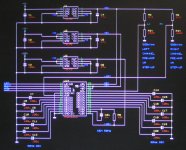
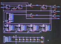
And now the practical 24 bit Left Justified to Simultaneous protocol converter circuit.
With LJ format the Right channel data is present when WS is low and the Left channel data is present when WS is high. With I2S the Left channel data is present when WS is low and the Right channel data is present when WS is high.
The 24 bit left justified interface signals DI (Data Input), WSI (Word Select Input), and BCKI (Bit Clock Input) enter the circuit at the top left.
First we have to identify and invert the MSBs. With LJ format we know that the MSB comes immediately after a WS change. U1, U2, and U9 create a delay that equals exactly one bit.
This works as follows, U1 delays the WSI signal for half a BCKI clock period. U2 receives an inverted BCKI signal and delays WSI for another halve BCKI clock period. Total delay is now -exactly- 1bit.
When we XOR this signal (U2 pin 4) with WSI we get a positive pulse the moment MSB occurs in the stream, immediately after a WSI change.
XOR gates can be used to invert a signal. When we put a "1" on the control input the signal on the other input is inverted. When we put a "0" on the control input the signal on the other input is not inverted.
When we XOR this pulse with the DI signal we can invert MSB only as the inversion only occurs during the short moment the MSB identifier pulse goes high. I combined two XOR gates by using a 3 input XOR gate. If this is a problem one can combine U2 Q output with WSI in a 74HC86 and then combine the output of this 74HC86 with DI using a second 74HC86 XOR gate. The output of that second XOR gate is connected to U3 D input.
Ok so we inverted MSB on the fly for both L and R channels.
We will need data delay circuits and in order to phase align both L and R channel data we start with flip-flop U3 so we can clock out both L and R channel data on the same BCKO clock edge.
We now have the DOR signal present on U3 pin 4.
The Left channel can now be aligned by adding 32 bit delay (U5 ... U8) and now we have DOL data on U8 pin 13.
The remaining thing to do is disabling DOL, DOR, and BCKO for the remaining 48 bits.
U4 is a counter that only counts when WSI is low (RST = 0) After 16 pulses its output Q4 (pin 5) goes high and when we NOR this signal with WSI we get a window signal that is only "1" when the 16 data bits are clocked out.
This window signal drives 3 AND gates U12, U13, and U14 that force these signals to "0" after the 16 bits have been clocked out.
The WSI signal is simply fed through and occurs at the output as the LEO (Latch Enable Output) signal that latches the TDA1541A outputs (simultaneous mode) on the -rising- edge of BCK.
The circuit consumes very little power, simple LED (L1) and diode(D1) shunt offer approx. 2.4V supply voltage (VDD) so we don't need attenuator circuits and we have low switching noise in the protocol converter circuit.
Attachments
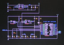
And here is the schematic for the matching SPDIF receiver configured for 24 bit Left Justified output.
Toslink IR receiver or S/PDIF pulse transformer can be connected to SPDIF in.
MCP120 is the reset circuit. Good reset circuit is -essential- to get SPDIF receivers working correctly. The MCP120 has open collector and requires an external pull up resistor.
LED L1 lights when the receiver is locked.
SCKO is set to lowest possible frequency in order to minimise on-chip interference.
The PLL loop filter has datasheet component values. Refer to datasheet for optimal loop filter placement and location of decoupling caps as this has major impact on (jitter) performance.
LP5907 ultra low noise LDO regulator is used for the 3V3 supply.
Attachments
- Home
- Source & Line
- Digital Line Level
- Building the ultimate NOS DAC using TDA1541A