I would continue to work on, but I don't know how to do all of these in LTSpice. The only simple mode works for me is 1K sine wave test). There is also no any usefull video on Youtube how to simulate amplifier in LTSpice
I have sent you a pm re doing this.
Here is a rig I made which can do square, sawtooth, sine and sine burst input as well as OLG measurement. It may be hard to use in LTSpiceXVII due to interface changes though...
Note that all waveform generators are turned on in that file for demonstration, IE sine=1, saw=1, square=1 etc.
Note that all waveform generators are turned on in that file for demonstration, IE sine=1, saw=1, square=1 etc.
Attachments
It looks normal but the FFT looks cleaner and the THD into 4R is 0.000000%. I must be missing a trick here - I don't think this is right.
In the test set up I have been using the result into 4R// a variety of test caps ranging from 1nF to 2u2 is between 0.000114-0.000118% bracketed figures 0.000174-0.00185%.
Being a bit of a cynic I even took those with a large pinch of salt and kept them to myself.
In the test set up I have been using the result into 4R// a variety of test caps ranging from 1nF to 2u2 is between 0.000114-0.000118% bracketed figures 0.000174-0.00185%.
Being a bit of a cynic I even took those with a large pinch of salt and kept them to myself.
The first .four result is an FFT of the input voltage, just to make sure your input is clean. Second result is output THD. Third result is THD with only the first 4 harmonics. In theory these harmonics are the most benign, so if your first THD result is much higher than the 4-harmonic THD, then you have a lot of high order harmonics and this is supposed to be bad. But you should make up your own mind, this is not supposed to replace a listening test.
The first .four result is an FFT of the input voltage, just to make sure your input is clean. Second result is output THD. Third result is THD with only the first 4 harmonics. In theory these harmonics are the most benign, so if your first THD result is much higher than the 4-harmonic THD, then you have a lot of high order harmonics and this is supposed to be bad. But you should make up your own mind, this is not supposed to replace a listening test.
If that is error log stuff everything is zero across the board in your test rig until the last reading of the four which comes out at 0.000272% bracketed figure 0.000312%.
The FFT of the circuit using Bob Cordell's test method at 20 Volts peak has high order harmonics between 10-20k that I don't like - the worst of them is - 96dB.
No celebrations there.
The THD function only works with sine input.
I can't really comment without knowing how you are trying to use it and what you are using it on.
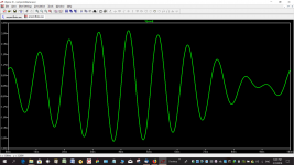
Sine at 1kHz then FFT then Error log.
I have tweaked the circuit a bit - reducing some values C34 and C35 (Vas) C14,C17,C5, and R18 (Output).
In a square wave tests I look at R20 ahead of the coil and the indications are the circuit is stable with a 4 ohm load and wide range of parallel test caps.
Unrealistically I have left them in the sine wave simulation attached - looking to see what is not to like there - even though in reality the load will be removed to the end of a length of speaker cable once any delay relay kicks in. You can delete the capacitors if that is more appropriate.
I modeled the emitter resistors as inductors with resistance of 0.47 ohms.
The odd values for the resistors in the output zobel are parallel combinations of low wattage film 0.6W types e.g. R18 is 5 off// 51 ohms.
For me this is a paper design so if the place for my simulation is the waste paper basket you can be blunt about it.
Attachments
Multi-emitter and ring-emitter power BJT specify the maximum fT. fT changes with collector current. It can be that a "high fT" power BJT has fT 30 MHz at Ic 2 amps but 100kHz at ic= 50 mA and ft 100 kHz at ic 8 amps. This holds also for base drive impedance close to zero. Makes compensation difficult . The original single diffused 2N3055 was rather easy to handle in terms of compensation as fT hardly varies with collector current
If power BJTs produce high fT of 100kHz or 30MHz this hasn't to be oscillation, just high fT output. Perhaps oscillations have different reasons than fT of power devices.
In the worst case can't the compensation be configured from 1A Ic for example, setting constant bias current point, than with higher Ic fT only be degrading while increasing the stability?
In the worst case can't the compensation be configured from 1A Ic for example, setting constant bias current point, than with higher Ic fT only be degrading while increasing the stability?
It makes compensation a try and error thing in case of global negative feedback loop. Some designers proposed nested feedback or even keep the power section completely out of global feedback. The simplest is compensation for lowest gain and phase shift according to lowest fT vs collector current, that is over compensationIf power BJTs produce high fT of 100kHz or 30MHz this hasn't to be oscillation, just high fT output. Perhaps oscillations have different reasons than fT of power devices.
In the worst case can't the compensation be configured from 1A Ic for example, setting constant bias current point, than with higher Ic fT only be degrading while increasing the stability?
It's worth repeating that because of this large change of fT with current, simulations using AC analysis do not show the variation in parameters. They only show the results for the situation usually with quiescent current conditions, as that tends to be the D.C. condition used to set the AC parameters. So what might work for quiescent conditions might no longer work in a Class AB design when the fT changes - hence we often see spurious oscillations in one half or the other or both at higher currents unless the feedback and compensation systems are robust, and have to be dominant so that transistor parameter changes cannot affect the stability.
One reason that the Miller compensation is widely used is because of its robustness. But it is not the best approach for the lowest distortion.
One reason that the Miller compensation is widely used is because of its robustness. But it is not the best approach for the lowest distortion.
AN approach that seems to work is to limit the input stages to two gain stages only - e.g. input differential and differential, Darlington VAS stage, with triplet output stages. Global NFB with phase lead from the output works with RC phase lag on the outputs of the differential input stage, and VAS output stage. However there may still be some slight, damped, internal ringing, which can be completely cured by taking the compensation from the VAS stage to the feedback point instead of the output connection. The 20kHz may increase to about 0.01% but THD is around 0.002% at 1kHz, lower if the global approach is used.
What can be the simplest and stable schematic for SE or preferably balanced input from our research here?
The Lazy Cat circuit is full complementary symmetry push-pull through every stage.
From what I can make of it the most straight forward compensation is to use the Miller method.
With this the added capacitance between collector and base reduces the frequency of one pole and makes it dominant while reducing another in magnitude and forcing it to a higher frequency - a phenomenon known as pole-splitting.
The output driver stage has some voltage gain whereas too many poles close together in frequency accelerates changes in phase which is bad for stability.
The method of taking the compensation from the Vas to the inverting input (John Ellis) is one I have used myself in other circuits - used here it makes my simulation unstable - the diversion of current to the inverting input I suspect causes the poles in the Vas and Driver stages to be too close together. In short the opposite effect of pole-splitting.
- Status
- This old topic is closed. If you want to reopen this topic, contact a moderator using the "Report Post" button.
- Home
- Amplifiers
- Solid State
- One of the Top Solid-State CFA amp design