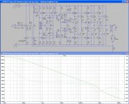
Sti show a front page power of 50W and the SOA graph confirms this up to ~ 15VceD44H11/D45H11 have quite bad SOA, for a 5W amp - maybe okay but I don't even
like them as drivers for a higher power amp:
https://www.onsemi.com/pub/Collateral/D44H-D.PDF
.6A at 30V = 18W for Onsemi, STmicro claims much better 1A at 30V:
http://www.st.com/content/ccc/resou...df/jcr:content/translations/en.CD00000942.pdf
Whereas the Onsemi version claims 70W on the front page, but when I look at the SOA graph I see it can only do that for single shot 1us
At 50% duty cycle & Tc<70degrees C, they show only 20W for the DC value upto ~15Vce.
I wonder how much worse it would appear if they had shown for 100% duty cycle DC?
The ONsemi datasheet contradicts itself and looks as though it might be wrong.

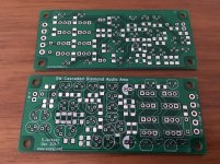
Promising so far. There's a stuff-up on the PCB where I forgot to link C7 to R3, but that's an easy fix as the pads are right next to one another.
Also I forgot to order 3V9 zeners, so I've substituted 6K2 resistors, making the clipping control not really right.
The board is stable so far with C3=330p, R10=1K, C6,7=22p, R22,23=1K, C8=22n.
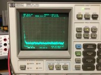
No load quiescent current is 78mA with +/-18V supply. There's a rather nasty 62mV DC offset - I guess I'm really going to have to match Q1 & Q2. Input referred noise measures at 4.2nV/rtHz.
Thus far I'm just driving a 50 Ohm load, as I haven't yet put a heatsink on.
(Very) preliminary 1KHz THD figures are:
1.25V - 0.00004%
1.77V - 0.00006%
2.50V - 0.00010%
3.53V - 0.00007%
5.00V - 0.00014%
7.07V - 0.00013%
10.0V - 0.00016%
Early days yet, but no burned fingers so far!
Also I forgot to order 3V9 zeners, so I've substituted 6K2 resistors, making the clipping control not really right.
The board is stable so far with C3=330p, R10=1K, C6,7=22p, R22,23=1K, C8=22n.
No load quiescent current is 78mA with +/-18V supply. There's a rather nasty 62mV DC offset - I guess I'm really going to have to match Q1 & Q2. Input referred noise measures at 4.2nV/rtHz.
Thus far I'm just driving a 50 Ohm load, as I haven't yet put a heatsink on.
(Very) preliminary 1KHz THD figures are:
1.25V - 0.00004%
1.77V - 0.00006%
2.50V - 0.00010%
3.53V - 0.00007%
5.00V - 0.00014%
7.07V - 0.00013%
10.0V - 0.00016%
Early days yet, but no burned fingers so far!
Attachments
That's low, very low !Promising so far............. Input referred noise measures at 4.2nV/rtHz...........
Is it topology, or devices selection, or resistances selection?
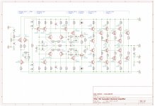
I used BC547’s in the input diffamp due to their reasonably low noise figure. I picked the input resistance of 200 ohms to minimise noise.
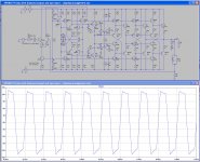
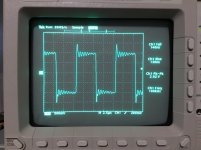
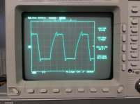
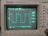
It’s been rather enjoyable playing with the compensation to improve stability. Running square waves in is useful, as I can straight away see slew rate and any ringing.
It’s been rather enjoyable playing with the compensation to improve stability. Running square waves in is useful, as I can straight away see slew rate and any ringing.
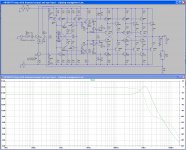
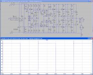
There's no such thing as a final .asc. The simulation that I have for the amp physically playing on my desk now is attached here.
I'm happy with the stability now - I can run the physical board (as opposed to the sim) happily at x6 gain (1K Rf) without issue - I tried x2 (200R Rf) but that was pushing the friendship, alas, and it was breaking into ringing a bit on the -ve half cycle. The sim is fine at x2.
Square wave response is good, with a little overshoot but nothing terrible. It's really nice on clipping.
Offset is still 60 odd mV, which I think is excessive - I'm confident that can be reduced with some first stage matching.
Attachments
-
 Screen Shot 2018-01-13 at 9.02.53 pm.jpg789.1 KB · Views: 537
 -
 Screen Shot 2018-01-13 at 9.06.56 pm.jpg812 KB · Views: 507
 -
 Screen Shot 2018-01-13 at 9.07.51 pm.jpg806.7 KB · Views: 513
 -
 Screen Shot 2018-01-13 at 9.09.26 pm.jpg665.7 KB · Views: 544
 -
 Screen Shot 2018-01-13 at 9.10.01 pm.jpg725 KB · Views: 580
 -
4W BD179 Amp with diamond output and npn input - clipping management.asc15.6 KB · Views: 89
-
5W Cascaded Diamond Amplifier.zip210.4 KB · Views: 104
Last edited:
That's low, very low !
Is it topology, or devices selection, or resistances selection?
These noise measurements befuddle me.
I just repeated the measurement, using at 8 ohm output load and shorting the input, with gain set at 20dB (x10).
Output referred my spec-an says 42nV/rtHz, so I make that 4.2nV/rtHz input referred. I double checked that the amp was actually connected. Indeed it is - shorting the input of the spec an gives 14nv/rtHz.
Attachments
Last edited:
R labels referring tot last pic?Why not adjust the offset simply by replacing R3, R4 with a pot. Once set, measure the pot and replace with fixed resistors.
Do not change R3 & R4.
Instead measure the unbalance across R3 & R4 and across R7 & R20 and across R8 & R21 and work out which transistor pair is causing the worst of the output offset.
The unbalance across R14, 15, 16 & 17 should also be a clue to where unequal currents are flowing.
Last edited:
As illogical as this might sound, the 2N5089 is not the comp for 2N5087 rather the 2N5210
is, I told Bob about this in the list on his SPICE web page but he has not bothered to fix it.
Look up the 5089 and you'll see that it has much lower Vceo and is optimized for higher beta:
https://www.onsemi.com/pub/Collateral/2N5088-D.PDF
I know this from spending countless hours as a kid working on various amps that used them,
Tigers, HK Citation, etc.
Here's an example from Bryston: http://www.bryston.com/PDF/Schematics/3B-8BST_SCHEMATICS.pdf
Last edited:
Thanks for that Pete - I'd assumed they were complements based entirely on their numbering - indeed I'm not sure if I've ever looked up the data for a 2N5087 - just assuming it's characteristics from the 2N5089 data.
It's not the 2N5087 I want a complement for - it's the 5089, with it's 50MHz Ft and 450 Hfe @ 1mA...
It's not the 2N5087 I want a complement for - it's the 5089, with it's 50MHz Ft and 450 Hfe @ 1mA...
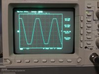
Here's the behaviour when clipping with a 47 Ohm load, also square waves at 10 & 100 KHz, 20Vp-p output (no input filtering) plus a 100KHz 1Vp-p output square wave to show small signal slew rate.
Attachments
... I want a complement for the 2N5089, with it's 50MHz Ft and 450 Hfe @ 1mA...
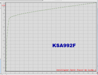
You might consider one of the attached. According to octopart.com they are both in stock at several distributors including Mouser.com and Digikey.com .
In my quick and dirty tests, the '992 had a higher Early voltage (flatter Ice vs Vce)
_
Attachments
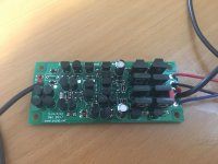
The idea for heat sinking is to bolt the inner two rows of transistors (these are the high-current ones) to a piece of aluminium T extrusion. I can use 2mm thick flat strip either side, one countersunk and the other threaded, to secure countersunk M3 screws.
About cooling, I saw this heatsink I planned to use before, maybe it can hold 2 boards, has a T profile in. Maybe too big. Im not sure if it is widely available, because I couldn't find the maker.
An externally hosted image should be here but it was not working when we last tested it.
An externally hosted image should be here but it was not working when we last tested it.
Double T sink would suit a pair of vertically oriented amp PCBs.
That arrangement brings the like for like terminals only 57mm apart.
This suits minimising voltage losses and minimises added inductance between the channels and can result in lower hum interference in the completed stereo amplifier.
That arrangement brings the like for like terminals only 57mm apart.
This suits minimising voltage losses and minimises added inductance between the channels and can result in lower hum interference in the completed stereo amplifier.
- Home
- Amplifiers
- Solid State
- Cascading diamond buffers - a cheap low THD 10W amp with TIP41C