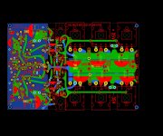
I've made the layout with ground plane in the input section on double-sided pcb. Instead of missing traces jumpers will be used. Is it done right? Any thoughts?
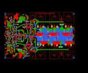
Second image is with top layer missing traces. Missing GND traces haven't shown.
Second image is with top layer missing traces. Missing GND traces haven't shown.
Attachments
Last edited:
Hi AndriyOL,
I assume you have familiarized yourself with the posted material on high speed layout design and ground plane concept. I would like to ask what your reasoning is to do only half the board e.g. input section with a ground plane ? Would you not want a small loop area for all signals on your board in particular those that carry large currents and therefor will have larger magnetic fields ?
I assume you have familiarized yourself with the posted material on high speed layout design and ground plane concept. I would like to ask what your reasoning is to do only half the board e.g. input section with a ground plane ? Would you not want a small loop area for all signals on your board in particular those that carry large currents and therefor will have larger magnetic fields ?
at audio frequencies low loop area has to be enforced by trace geometry - pairs, power/gnd bus interleaves
this is most important when you have Class B output Q and PS rectifier/cap nonlinear currents
in the frontend a gnd plane is convenient, the diffusing of the currents only gives tiny gain differences when they are all Class A and small
this is most important when you have Class B output Q and PS rectifier/cap nonlinear currents
in the frontend a gnd plane is convenient, the diffusing of the currents only gives tiny gain differences when they are all Class A and small
Last edited:
Hi Kct.Hi AndriyOL,
I assume you have familiarized yourself with the posted material on high speed layout design and ground plane concept. I would like to ask what your reasoning is to do only half the board e.g. input section with a ground plane ? Would you not want a small loop area for all signals on your board in particular those that carry large currents and therefor will have larger magnetic fields ?
Yes, I've read it.
I did gnd plane on input section only to avoid couple the high current output stage to the input stage, which may change the potential and cause oscillations.
Do you offer to create another gnd plane after the 10R for the output stage?
at audio frequencies low loop area has to be enforced by trace geometry - pairs, power/gnd bus interleaves
Do you mean multilayer pcb will be better or gnd plane for full layout?
Last edited:
On a two-sided board there is often not enough space to do a full ground plane without increasing the power stage loop area by large amounts. Since the ground plane only starts working at 5KHz or so, the increased loop area of the power traces will result in more distortion than if the traces were routed intelligently without a ground plane to minimize current loops and cancel fields.
Hi, AndriyOL,
In low frequency audio application, as long as we follow the basic theory, I don't think we need multi layer PCB or even a ground plane. Thick trace only needed for high current trace when PSU is on board.
Why have you focused on the layout when the source of the oscillation is still unknown? If you follow the basic theory on the layout implementation and the amp still oscillates, the design is simply unacceptable imho. In your spice analysis you should have shown the Nyquist stability criteria (I think I haven't seen one).
Let me digress. Every time I have thought that oscillation might be caused by a layout issue, except for once on someone else's board, it has turned out the problem was something else, sometimes a miswire. Do you have your PCB linked with a schematic so it will keep you from making errors?
Doug Self has a lot of experience, if he gets good performance without ground planes, then your problem can't be because you didn't use a ground plane. Make sure that the layout matches the schematic first of all.
On your latest layout the PSU cap return currents will pollute your feedback signal. This is something you need to get right before trying to use ground planes. It would be better if your output/ground points were right next to the 16 ohm resistor, so there are no more connections getting between them and the feedback point.
BUT, again this is not the kind of error that causes oscillation. It's quite possible there is something wrong with the simulation and you built a faulty circuit without realizing this.
I confirm, I traced a pcb of the preamplifier RIAA of D.Self (Elektor 2012) without ground plane and this circuit is totally silent and "cherry on the cake" it is of a superb sound.Doug Self has a lot of experience, if he gets good performance without ground planes, then your problem can't be because you didn't use a ground plane. Make sure that the layout matches the schematic first of all.
")
Attachments
A common technique on low frequency power boards is broadside routing for high power pairs. That is one wide track on the top, with the return routed directly underneath it. This gives a low impedance path for the current delivery with tightly coupled fields, minimising the effect on other signals and return paths. A ground plane for low frequency power can be counter productive. On multilayer designs where we will use more than one pair if required for current delivery or a low impedance/low voltage drop path for higher switching circuits.
Hi Kct.
Yes, I've read it.<snip>
Hi AndriyOL,
see, what I do not understand is that you want to apply the new knowledge you gained from the papers to only half of the board.
Yes, I mean ground plane under the entire board is better.
Consider, you have reduced the loop area of your input section by putting the ground plane underneath, this is good and it will make your input section less receptacle to electromagnetic stray fields. Great.
But what about the possible source of unwanted electromagnetic stray fields, e.g. the high current section of your design. If you were to leave it as is, you would still have large loop areas on these traces and so you would allow the 'love' to spread to nearby traces and cause grief.
For the point I am trying to make, I am sure you have heard of the concept of loop antennas. If not feel free to google. Yes, I mean RF antennas. As with RF antenna application you generally have a receiving antenna and a transmitting antenna. (lets imply these antenna are loop antennas for the point I am trying to make)
Now if you have two very good such antennas (RX and TX), your 'RF system' works very well as you can receive a signal that is transmitted from far away.
Btw. good loop antennas have large loop areas.
In audio application, I believe it is not desirable to have 'build in' loop antennas in the design which could possibly radiate or receive signals, the amplifiers very own signals perhaps. Therefore it may be best to avoid any structures in the design that make loop antennas.
E.g. we want the smallest possible loop area to achieve at best a very very poor loop antenna on the 'receiving' as well as 'transmitting' side..
This is where we bring copper e.g. ground plane as close as possible underneath the traces above. This results in the smallest possible loop area between the trace(forward path) and ground (return path). With a small loop area there is very little electromagnetic fields which could possibly enter or escape between the forward path and return path and so we have achieved a very poor 'loop antenna' action.
Afterall, we do tend to twist wires to get them as close as possible to each-other. There is a reason for this, it is not only the 'neat factor' but so we minimize the loop area between them. Does this make sense to you ?
Let me ask you this, what do you think happens when an amplifier -magically- 'transmits' and 'receives' its own signal and amplifies it ?
btw. Happy Holidays
Hi AndriyOL
Common Base Stages are the fastest form of an amplifier. This can become a very high frequency stage oscillator. You have several stages that can be the problem. Adding BASE impedance of a several ohms will stop any high frequency oscillation. If the base has a big cap to ground or to PS add a base resistor. You have several stages that meet this condition.
I would first get a spectrum analyzer and see what frequency is. I have had some problems with a 50-200MHz on the inputs to the VAS.
Good hunting Duke
Why have you focused on the layout when the source of the oscillation is still unknown? If you follow the basic theory on the layout implementation and the amp still oscillates, the design is simply unacceptable imho. In your spice analysis you should have shown the Nyquist stability criteria (I think I haven't seen one).
I followed the advices of more experienced people than me.
I've been told that according to scope pictures, there are 2 oscillation modes: one around 4Mhz which is the global NFB loop, another around 80Mhz which is output stage local feedback or VAS local feedback.
I'm not completely sure if the layout implementation is correct and isn't a source of oscillation.
I would definitely do, but how can I show Nyquist stability criteria?
Hi, AndriyOL!
To prevent oscillations, try reducing the value of R45 to 4.7 ohms, or even 3.3 ohms.
I will try, but can it cure the source of oscillation?
Do you have your PCB linked with a schematic so it will keep you from making errors?
On your latest layout the PSU cap return currents will pollute your feedback signal. This is something you need to get right before trying to use ground planes. It would be better if your output/ground points were right next to the 16 ohm resistor, so there are no more connections getting between them and the feedback point.
BUT, again this is not the kind of error that causes oscillation. It's quite possible there is something wrong with the simulation and you built a faulty circuit without realizing this.
SL6 I used for layout doesn't have such feature. But I had checked it before making pcbs. Will check it again.
I'll try to redesign so there will be clear path between feedback input and speaker out/gnd connections. Thanks.
Nobody completely sure if the circuit is faulty or not. Simulation with basic components can be done, according to other members, if I'm not wrong.
Last edited:
One thing I suggest is for you to do is use 2 10x probes with 10pF capacitors at the ends in differential mode with your scope, and probe each B-E junction to see which transistor is oscillating the most. That could be a significant clue where the problem is.
I'm stll not very good familiarise myself with the scope functionality. Could you please advise how to set the scope in differential mode?
Could the oscillation be due to fake or mismatched 2sc3423/2sa1360 transistors? They have approximately 150/200 hfe as complementary pair, I bought them from Mouser some time ago.
Hi AndriyOL,
see, what I do not understand is that you want to apply the new knowledge you gained from the papers to only half of the board.
Let me ask you this, what do you think happens when an amplifier -magically- 'transmits' and 'receives' its own signal and amplifies it ?
btw. Happy Holidays
It's not possible to make good gnd plane for double sided pcb. Than I have to go with 4 layer design. However in any way gnd plane has to be divided by two parts through 10R.
You are right, it's oscillation effect.
Thanks. I wish Happy Holidays you too and all diyaudio members ).
Last edited:
Mismatched transistors don't cause oscillation except once every 200 years. Transistors haven't existed for more than 100 years so it hasn't happened yet.
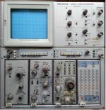
Another thing to try, take a 10x probe and just wave it over the PCB, see if you can find the area that emits the most 80MHz noise through the air. I haven't used a lot of scopes, but I may be able to tell you what to do if there was a detailed photo of your scope.
Cascodes like in your input stage can occasionally oscillate.
Last edited:
Okay, forget all this. The circuit as posted in the first post won't work.
Putting a second input pair on a CFA will not work as a negative input, although it would be nice if it did.
If you had at least started with a working simulation and altered it to develop your amplifier you would have started with a circuit that could in principle work. But not only did you not take advantage of the simulator to check your work, but you didn't even faithfully reproduce your schematic when making your PCB.
No one expected the problem to be this bad, which is why after all this time and the opinions of many experts no one realized the problem.
I hate to bring the bad news, but look at it this way. You no longer have to spend any more of your or anyone else's energy on this circuit. Instead you might be able to get started on the right path and finally do what you had originally intended to do.
Mismatched transistors don't cause oscillation except once every 200 years. Transistors haven't existed for more than 100 years so it hasn't happened yet.
Another thing to try, take a 10x probe and just wave it over the PCB, see if you can find the area that emits the most 80MHz noise through the air. I haven't used a lot of scopes, but I may be able to tell you what to do if there was a detailed photo of your scope.
Cascodes like in your input stage can occasionally oscillate.
The problem with this method is I see an oscillation on the scope in an air. Please check the post 16.
Here is the photo.
I would simulate it if I had a models of all transistors.Okay, forget all this. The circuit as posted in the first post won't work.
Putting a second input pair on a CFA will not work as a negative input, although it would be nice if it did.
If you had at least started with a working simulation and altered it to develop your amplifier you would have started with a circuit that could in principle work. But not only did you not take advantage of the simulator to check your work, but you didn't even faithfully reproduce your schematic when making your PCB.
No one expected the problem to be this bad, which is why after all this time and the opinions of many experts no one realized the problem.
I hate to bring the bad news, but look at it this way. You no longer have to spend any more of your or anyone else's energy on this circuit. Instead you might be able to get started on the right path and finally do what you had originally intended to do.
I already tried as SE, but the amp had the same issue.
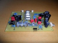
I'm sure the layout corresponds to the schematic. I've checked it before the production. There were only silkscreen mistakes, but not in a copper layout.
What do you mean the right path is?
Attachments
Last edited:
Hi AndriyOL
Common Base Stages are the fastest form of an amplifier. This can become a very high frequency stage oscillator. You have several stages that can be the problem. Adding BASE impedance of a several ohms will stop any high frequency oscillation. If the base has a big cap to ground or to PS add a base resistor. You have several stages that meet this condition.
I would first get a spectrum analyzer and see what frequency is. I have had some problems with a 50-200MHz on the inputs to the VAS.
Good hunting Duke
Hi Duke,
These several stages are common base bridges of input transistors and second VAS transistors?
Do you mean base impedance to ground or as base stopper?
Isn't it possible to determine the frequency by oscilloscope?
- Status
- This old topic is closed. If you want to reopen this topic, contact a moderator using the "Report Post" button.
- Home
- Amplifiers
- Solid State
- One of the Top Solid-State CFA amp design