Kasey197 thanks for your response.
Well, it says in the manual that there are two pairs of complementary input JFets.
There are many advantages to parallel-coupling JFets at the input.
Although - as you correctly pointed out - that is not necessary to drive the 2nd stage transistors.
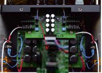
A picture of the internal pcb of the XA25 would be very helpful.
However, I believe the main circuit to be (conceptually at least) very close to the last version I submitted.
As for the shutdown and bias generator, these would not be difficult to duplicate.
cheers
Well, it says in the manual that there are two pairs of complementary input JFets.
There are many advantages to parallel-coupling JFets at the input.
Although - as you correctly pointed out - that is not necessary to drive the 2nd stage transistors.
A picture of the internal pcb of the XA25 would be very helpful.
However, I believe the main circuit to be (conceptually at least) very close to the last version I submitted.
As for the shutdown and bias generator, these would not be difficult to duplicate.
cheers
Correct It wil look more like the Sony VFET frontend, even the number of resistors are the same as which I count on the PCB ")
The interesting and unknown part is this:
"The removal of this form of feedback is an important element in the performance of the XA25 and is accomplished by new approaches to stabilizing gain and bias of push-pull FETs.
This gives a lower output impedance, more gain, and lower spectral content of distortion, as evidenced by measurements (see the specs section), but the more important factor is the difference it makes to the music."
Kasey197 thanks for your response.
Well, it says in the manual that there are two pairs of complementary input JFets.
There are many advantages to parallel-coupling JFets at the input.
Although - as you correctly pointed out - that is not necessary to drive the 2nd stage transistors.
A picture of the internal pcb of the XA25 would be very helpful.
However, I believe the main circuit to be (conceptually at least) very close to the last version I submitted.
As for the shutdown and bias generator, these would not be difficult to duplicate.
cheers
There are two pairs in a stereo amp
----------------------------------------------------------------Higher PSU voltages might spell doom for the small JFETs, since the 2SJ74 has a maximum reported Vds of 25V. ZM's suggestion that the JFETs, and not the second stage MOSFETs, are cascoded is almost certainly correct, since this is how the other Pass Labs X series products are built. In fact, I think Pass himself confirmed this in one of the threads and said that the cascoded MOSFET statement was a misprint. The cascode devices are likely his usual choice of bipolars: 2SC4793 and 2SA1837. See the Sony VFET2 front end, which is a more elaborate BA3.
I think you (and Zen Mod) are right.
Looking at the Pass Labs Front End arsenal, they certainly use the Cascoded JFets along
with Common-Source connected 2nd stage Voltage amplifier stage.
I do not see why they would want to alter this. However it clearly says "cascoded Mosfets", so do you
think the second stage would also be cascoded?
And you are of course right about the Vds max of input JFets. I also read the comment made by Mr Pass about the misprint.
Well, take a look at this:

Last edited:
There are two pairs in a stereo amp
Hmmm.... I dont know... why would they say it this way? It is quite confusing.
But it is an interesting thought.
What about this:
Attachments
What about this:
That is the basic circuit we arrived at in the F4 Beast thread. The real trick, as others have said above, is figuring out the bias mechanism...
However, there is no mention of cascoded input JFETs in the manual, but the online manual clearly states cascoded Mosfets:
That is a typo.
-------------------------look at this....
That's good.
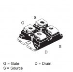
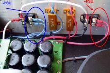
Well:
1- the big devices are the output MosFets
2- the devices on the small thermal heat-sinks on the main PCB are either the cascode transistors for the 2nd-stage, or the 2nd-stage gain transistors themselves.
3- between the pots, there are two additional big transistors in TO-220 or TO-126 packages, I would assume THESE are the second stage gain transistors.
You are referring to the enlarged section of the picture, showing possibly the input JFets, and the two large black transistors might be the cascode devices of the input stage.
What about the second stage? Do you think it is cascoded??
That is a typo.
Thank you Mr Pass for your response.
Ok, so the Input Stage is a pair of Cascoded JFets, but what about the second stage? Are they Cascoded?
That is the basic circuit we arrived at in the F4 Beast thread. The real trick, as others have said above, is figuring out the bias mechanism...
------------------------------------
Thanx for your response.
The picture sent by Walter shows what kinda looks like 4 transistors, that is two pairs.
I went through the F4 Beast thread, and although the basic circuit uses the same arrangement
of devices, it is quite different than the picture I presented above.
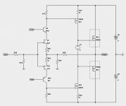
OK... please take a look at this.
Lose R21-24 since degeneration should be eliminated from all stages, per the user manual.
What do we know about the output devices? and of course the input devices?
Input JFETs: 2SK170/2SJ74
Cascode devices: 2SC4793/2SA1837
Second stage MOSFETs: 2SK2013/2SJ313
Output MOSFETs: IXYS somethings - see F4 beast thread for our guesses
Lose R21-24 since degeneration should be eliminated from all stages, per the user manual.
Input JFETs: 2SK170/2SJ74
Cascode devices: 2SC4793/2SA1837
Second stage MOSFETs: 2SK2013/2SJ313
Output MOSFETs: IXYS somethings - see F4 beast thread for our guesses
---------------------------------------
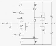
OK, I updated the schematics with the transistors.
The output transistor suggestions in the F4 Beast thread is a little uncertain.
I am not sure these are the devices used. However I included them.
Take a look at this:


...
Cascode devices: 2SC4793/2SA1837
...
our guesses
Unfortunately 2SC4793 and 2SA1837are no longer available.
- Home
- Amplifiers
- Pass Labs
- Pass XA25?