I don't think we are near finite limitations on switching time. The limitations we are facing are due to extra base currents that are not directly proportional to collector currents. What about these cannot be modeled with LRC?
If they can be modeled with LRC then they can be compensated by LRC.
Also think about it this way. Normal EF output stages have no problems with switching time. So the problem with current-driven outputs must be because of the base current behavior.
Base current from Cbc is 90 degree phase shifted, easy to compensate as long as the capacitance doesn't change too much at the crossover point. If the load has extreme phase shift it may move the crossover point closer to the rails, which would change Cbc. If this turns out to be a problem then it may be necessary to use a vegetative BJT to track the capacitance, or perhaps a normal diode with a variable current mirror ratio.
Base current due to Cbe is dependent on Ic and can have phase shift above 90 degrees, two things which make it highly problematic. Any compensation must be referenced to output current, and must mimic the dramatic rise in phase shift at low currents, as well as the Vbe-dependence of the capacitance. The more I experiment with this the more I realize it will be extremely difficult if not impossible to effectively compensate this.
Cordell's model has Tf (forward transition time) for the MJE15032 set at 3.8nS.
Then how can we reduce distortion at 1kHz and 20kHz?
Heavily switched-up circuits like this are a pain when it comes to optimizing feedback. Often times you will find that to keep one part happy you need a miller cap in a certain place, but putting a miller cap there ends up sabotaging the rest of the feedback loop. So you can try splitting it into a two-pole miller cap, or perhaps a local transitional miller cap, or some other on the fly compensation, but you can rarely fully eliminate the contribution that part makes to distortion in the audio range.
Then there is the problem that the positive half of the output stage may have a different slew rate than the negative half. Or maybe the negative half is 10 times slower - then you have to lower the ULGF by 10 times while gaining lots of THD at high frequencies.
That said, the main thing limiting the linearity of this amp are the stability compensation and the DC gain of the output stage. With both of these problems solved you could get much lower distortion. But due to the clunky nature of this output stage, you need to be very careful at each step to make sure that the amp has acceptable overload behavior and doesn't latch, otherwise you may spend too much time working on something that is not rugged enough for real life use.
If you want to try another direction, maybe you could gain some inspiration from the Circlophone:
http://www.diyaudio.com/forums/solid-state/189599-my-little-cheap-circlophone.html
I had the thought earlier today that it may be a good concept to adapt to current drive. It is not so clunky that the feedback loop can't be reasonably fast.
Last edited:
Hi Keantoken,... So the problem with current-driven outputs must be because of the base current behavior.
...
Cordell's model has Tf (forward transition time) for the MJE15032 set at 3.8nS.
Bear in mind the Beta starts to roll off with frequency from FT/Beta -- for the MJE15032 (it's the same Tf value for the MJL3281) so fb = 40MHz/160 = 250kHz.
With current drive it's the Beta that determines LF linearity, and fb -3dB determines the amount of nfb that we can apply at 20kHz and THD at 20kHz.
So we are now actually using very slow power transistors, even though they appear to be very fast -- they are only very fast if they are voltage driven.
I think that's the reason we can't apply as much negative feedback at 20kHz as voltage driven output stages. And if that is the case then maybe I need to consider a Circlophone © ♫♪ (as you suggested in your other post).
So I'll stop trying to get Wim's amp distortion down further and now concentrate on my Linear Audio V13 CSD amp -- to see what can be done to reduce the cross conduction current with minimal extra circuitry.
Anyone is still welcome to look at ways to get Wim's amp distortion down at 20kHz. Maybe there's be a better form of compensation?
Cheers
Hi Ian,
Franscis Brooke (by the way, he is a Diyaudio member as FrancisBr ) made a simulation of Wim's circuit
http://www.diyaudio.com/forums/solid-state/302736-current-driven-ops-2.html#post4965229 (R16 and R17 are not present in the original schematics)
with the following results http://www.diyaudio.com/forums/soli...s-ab-output-stage-topologies.html#post2560979 .
If I remember correctly, he suggested to replace the input transistors Tr1 and Tr2 by Sziklai pairs to lower the distortion.
Anyone is still welcome to look at ways to get Wim's amp distortion down at 20kHz. Maybe there's be a better form of compensation?
Franscis Brooke (by the way, he is a Diyaudio member as FrancisBr ) made a simulation of Wim's circuit
http://www.diyaudio.com/forums/solid-state/302736-current-driven-ops-2.html#post4965229 (R16 and R17 are not present in the original schematics)
with the following results http://www.diyaudio.com/forums/soli...s-ab-output-stage-topologies.html#post2560979 .
If I remember correctly, he suggested to replace the input transistors Tr1 and Tr2 by Sziklai pairs to lower the distortion.
...My own Godzilla experiments was really a searching for a very simple solution that only had two stages. ... I don't expect you to spend any time with this issue anymore.
My apology for appearing to exclude discussing current-drive in your "Godzilla" amp in this thread. I can discuss it further in your "Godzilla" thread.
I am an advocate for simple amps and limiting them to 2 stages. I published a simple single stage Square-law Class-A amp in Linear Audio Vol. 1 -- it uses only 3dB on feedback, and that is optional, so it can be run as a true zero feedback amp. You can PM me for details.
And my Cube-law amp in Vol.8 and updated version with bipolars Vol.13 are two-stage amps.
In your "Godzilla" amps you are doing all the right things to maximise the benefits of current drive of the output stage; first by using a single pair for the output stage (no Darlington or CFP), and second by using a cascode for the VAS, and third, not using any input stage. For amps optimised for voltage driven power stages you do the opposite: Darlington (or Triple), don't cascode the VAS, and use an input stage, then take great care with compensation. With a 2-stage amp compensation is dead easy and very stable.
For current drive you should choose power transistors with an IKF parameter value at least 10 times the peak current (for normal 8 ohms load) to minimise beta fall at high currents for less HD3. Also match the betas within 20% for minimum HD2. Apart from the well known MJL3281 we now have the FJL4315OTU (aka 2SC5200) and FJA4313 and MG9410 all with low beta fall with current, and they are not expensive.
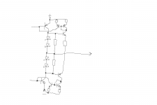
I have no access to LTSpice at the moment, so I don't know exactly what circuits have already been proposed, but what about the attachment? It is just a rough idea, I haven't tried to dimension, build or simulate it.
It's basically a class-(A)B control loop, but depending on how you dimension it, you can make it kick in only when cross conduction gets too high because of high frequencies if you like. The idea is that when only one side of the output stage conducts, the voltage across two Schottky diodes should be too small to make the rightmost transistors conduct. When the other side also conducts, the voltage can become large enough to turn on the rightmost transistors and the current mirrors, which will then turn reduce current through both halves of the output stage.
It's basically a class-(A)B control loop, but depending on how you dimension it, you can make it kick in only when cross conduction gets too high because of high frequencies if you like. The idea is that when only one side of the output stage conducts, the voltage across two Schottky diodes should be too small to make the rightmost transistors conduct. When the other side also conducts, the voltage can become large enough to turn on the rightmost transistors and the current mirrors, which will then turn reduce current through both halves of the output stage.
Attachments
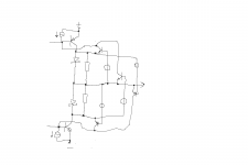
This is another untested wild idea. The transistors on the left are the output stage transistors, the resistors are small-valued current sensing resistors and the Schottky diodes are only there to limit the voltage drop across the resistors when the current is very high.
When the current through either side of the output stage gets too small, the current through one of the extra NPNs and one of the extra PNPs will increase and this will increase the current through both output devices. The opposite happens when the current through both sides gets too large.
By using transistor arrays for the extra transistors and their voltage sources (these can be implemented as diode-connected transistors with a small resistor in series, fed by a current source), the sense voltages in the crossover region can be kept as small as a couple of kT/q. The transfer from one side to the other then becomes quite smooth.
Attachments
Perhaps this is off topic, but I will only say one thing about current driven amplifiers. Or more precisely, my own domesticated version - the Baby Godzilla.
It uses the same cascoded VAS but with a high gm mosfet. This makes the VAS behave as it actually has around 50 ohm of output impedance ( in this particular case ).
So my B. Godzilla actually is voltage driven.
Ian, you haven't commented the thing a bout that H3 boost in current drive ( which is quite on topic )
Hi Keantoken,
Bear in mind the Beta starts to roll off with frequency from FT/Beta -- for the MJE15032 (it's the same Tf value for the MJL3281) so fb = 40MHz/160 = 250kHz.
This is exactly what I mean when I say the base is shunted by Cbe and Cbc. Real parasitics that can be probed and understood. How can we understand the Hfe rolloff if not by the parasitics that cause it? But it is not a physical limitation like Tf.
So we are now actually using very slow power transistors, even though they appear to be very fast -- they are only very fast if they are voltage driven.
Because voltage drive overcomes the Ic-dependent, 2nd order and highly nonlinear current through Cbe. Not through space-time portals or other impenetrable physics jargon, but through Cbe, a parasitic that we can know and understand. We probably can't compensate it, but at least we can know why.
BTW, notice that at RF, Jager's output stage IS essentially voltage drive. I can get 20KHz distortion down to 0.014%, still not very competitive.
I have no access to LTSpice at the moment, so I don't know exactly what circuits have already been proposed, but what about the attachment? It is just a rough idea, I haven't tried to dimension, build or simulate it.
I think many aided-switching ideas fall into the trap of trying to fix a crossover blip by adding more parts that are switching. You end up getting a drive current that is not proportional to output current and contains all the currents of the transistors switching on and off. Even if you do succeed in improving switching of the output transistors, the frontend has to deal with all the new switching harmonics and somehow come out on top.
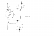
Your first schematic may not suffer from this since the correction current flows from rail to rail without modifying the current gain of the output stage. But you still must use switching drivers, because the output transistor base nodes have no way of dealing with reverse current.
I tried your second schematic in simulation without the two rightmost transistors and it did work, provided the drivers still did the switching. But you still have 2 extra transistors switching on and off.
Your third schematic looks worth a try, but I think it would be best to change the input transistors to look like the driver part of a diamond buffer. That way you get more current gain to suppress the extra switching harmonics.
Last edited:
I think many aided-switching ideas fall into the trap of trying to fix a crossover blip by adding more parts that are switching. You end up getting a drive current that is not proportional to output current and contains all the currents of the transistors switching on and off. Even if you do succeed in improving switching of the output transistors, the frontend has to deal with all the new switching harmonics and somehow come out on top.
That's why I like class-(A)B bias loops with a smoothly working non-linear network rather than an abruptly working non-linear network. I think the first of the three circuits is the worst in this sense. The other two can work quite smoothly when you design for a DC bias voltage of only a few kT/q across the resistors.
Your first schematic may not suffer from this since the correction current flows from rail to rail without modifying the current gain of the output stage. But you still must use switching drivers, because the output transistor base nodes have no way of dealing with reverse current.
I tried your second schematic in simulation without the two rightmost transistors and it did work, provided the drivers still did the switching. But you still have 2 extra transistors switching on and off.
Thank you for trying it! With the two rightmost transistors included, the impact on the distortion should be smaller because they compensate for the distortion of the two transistors to the left of the rightmost transistors - or at least that's the oversimplified first-order theory.
Your third schematic looks worth a try, but I think it would be best to change the input transistors to look like the driver part of a diamond buffer. That way you get more current gain to suppress the extra switching harmonics.
Sounds interesting, but I don't understand what you mean. Could you draw a sketch of the schematic?
Hi Marcel,That's why I like class-(A)B bias loops with a smoothly working non-linear network rather than an abruptly working non-linear network. I think the first of the three circuits is the worst in this sense.
Thanks for this. I am a fan of yours and often quote a section from one of your books about 15dB being the amount of negative feedback that changes a soft clipping amplifier to a hard clip sound. Google books will display the text on p161 here. I found the same level on a MOSFET amp before I read your figure and I mention this in my Cube amp Supplement (p19-20) here.
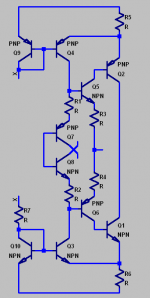
Your first circuit could possibly be improved by using Edmond Stuart's autobias error amp here.
Optoisolator U1 appears to be for under bias so it's not needed for our purposes. Instead connect U1 diode in series with U2 and then the transistors can be used to remove base charge. This would not discriminate between the power transistor that is on and the one that needs to turn off faster but probably that may not matter much. Probably, the extra circuitry needed to discriminate between the two output transistors may not be worth the effort.
Cheers,
Ian Hegglun
Last edited:
Using more feed back
Double pole compensation as suggested by Mr Self is worth considering. That something I will pursue. (Actually I want to also try it with Rod Elliot's P3A which has quite high distortion at 20 KHz with a relatively low amount of feedback).
I think that's the reason we can't apply as much negative feedback at 20kHz as voltage driven output stages.
Cheers
Double pole compensation as suggested by Mr Self is worth considering. That something I will pursue. (Actually I want to also try it with Rod Elliot's P3A which has quite high distortion at 20 KHz with a relatively low amount of feedback).
Hi Marcel,
Thanks for this. I am a fan of yours and often quote a section from one of your books about 15dB being the amount of negative feedback that changes a soft clipping amplifier to a hard clip sound. Google books will display the text on p161 here. I found the same level on a MOSFET amp before I read your figure and I mention this in my Cube amp Supplement (p19-20) here.
Hi Ian,
You are mixing me up with Menno van der Veen (-; I always use lots of feedback and no soft clipping, but I also include clipping LEDs to make sure the amplifier isn't driven into clipping.
Your first circuit could possibly be improved by using Edmond Stuart's autobias error amp here.
Optoisolator U1 appears to be for under bias so it's not needed for our purposes. Instead connect U1 diode in series with U2 and then the transistors can be used to remove base charge. This would not discriminate between the power transistor that is on and the one that needs to turn off faster but probably that may not matter much. Probably, the extra circuitry needed to discriminate between the two output transistors may not be worth the effort.
Cheers,
Ian Hegglun
Actually I think it is better to draw current from both bases, as this cancels the injected distortion to some extent.
The speed of the optocouplers might be an issue, I'm not sure what that will do to loop stability. In Edmond Stuart's version it doesn't matter because he makes the loop very slow with capacitor C3.
Best regards,
Marcel van de Gevel
Sounds interesting, but I don't understand what you mean. Could you draw a sketch of the schematic?
Attachments
Hi Marcel,Hi Ian,
You are mixing me up with Menno van der Veen (-;
Sorry. My apology! It's a sign I need to slow down a bit.

Thanks again for helping on this thread problem.
Cheers, Ian Hegglun
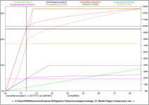
Here it is, one '.asc' sim-file and an picture showing (near) -200dB @ 1.4V input
To make this complete, here a set of graphs that shows the effect of the MosFet clipper, all voltages are in RMS, the horizontal straight lines are (top to bottom)
1) red) Amplifier clipping point (at extreme overdrive [input signal over 9Vrms] the amp still clips)
2) light green) 100W, this is the 'advertised' amplifier maximum power
3) dark green) Amplifier output voltage no longer linear (clipper on)
4) ochre yellow) Amplifier output power no longer linear (clipper on)
5) blue) Line-stage(pre-drive) clipping (clipper off)
6) purple) Line-stage(pre-driver) no longer linear (clipper on)
Graphs made in simulation while I do not have the equipment to do this in actual measurements.
Attachments
Last edited:
There is a problem. Your MOSFET models omit both subthreshold conduction and junction capacitance. So your MOSFETs don't show any conduction until 1.825 volts, which is incorrect, and is probably giving you excessively good results. If you have VDMOS models, they can be augmented with ksubthres=0.15 for a crude sanity-check to see the effect of subthreshold conduction.
Last edited:
- Status
- This old topic is closed. If you want to reopen this topic, contact a moderator using the "Report Post" button.
- Home
- Amplifiers
- Solid State
- Current-Source-Driven-power-transistors-and-mitigating-cross-conduction-distortion