the amplifier stability changes when the output reactance changes.
We can make the stability "safe" when there is no load attached and when there is a resistive load attached.
But when a reactive load is attached the stability margins change. In the extreme this can make the amplifier oscillate into destruction.
A much milder form of instability is overshoot on fast transients.
To see what effect reactive loading has on an amplifier, we do a 1kHz squarewave test.
The results are usually disappointing.
So we add in the Thiele Network. This helps stabilise the amplifier by providing a high frequency load (C+R) and partially isolates a changing reactive load (given by cables and speakers).
The L||R part of the Thiele Network Places a resistor damped air cored inductor into the output before it reaches the speaker terminals. The inductance is what helps isolate the cable and speaker load from the amplifier.
Very few power amplifiers work well without the inductor. Many new Builders do not fit this inductor and complain that the amp does not sound nice after longer listening sessions, or that all the ladies voices sound spitty/sibilant.
Thank you for info.
I am adding Thiele Network in the build.
Remove C1 & C10
Remove C25 & C26
Experiment with C3. Maybe as high as 1nF. Small steps, 330pF, 470pF, 680pF
R4 may need to increase, maybe higher than 10r.
Add L||R between output and speaker terminals.
replace D5 & D7 with power diodes. Try 1n4001 or similar.
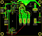
Here is my modified layout for the change:
- Removed C1 & C10
- Removed C25 & C26
- Experiment with C3 will be easy.
- R4 up to 10R.
- Added L // R = 3R3 // 0.5u between ouput and speaker terminals.
- Replaced D5 = D6 = 1N4001 <- Could you tell me the reason for this change?
- I also added two 1N4001 parallel with feedback capacitor to protect it.
Attachments
I see you have added inverse parallel diodes across C4. These can be fast signal diodes. 1n4148, or 1n914.
Some have suggested that the turn on voltage of a single diode might be a bit low and cause distortion of the wanted signal. If you agree, then you can use two diodes in series to replace ONE of the single diodes. The one to replace is that which has the correct forward voltage that matches the small DC voltage applied across the polar electrolytic.
The current through the diode (or pair of series connected diodes) in the worst case is full output voltage across the combination of Upper NFB + Lower NFB + capacitor. If the cap is shorted the worst case current would be Vpkmax / sum(upper+lower resistors). Typically this would be less than 2mApk for a 50W VFA amplifier. 75mA rating of a signal diode is many times greater than this. The worst case forward voltage would be ~2Vf and the worst case reverse voltage would be ~1Vf.
The diode in the reverse direction only sees and needs to limit that reverse voltage in a failure mode, when there is no useful signal at the output. This can remain as a single diode.
Last edited:
I see you have added inverse parallel diodes across C4. These can be fast signal diodes. 1n4148, or 1n914.
Some have suggested that the turn on voltage of a single diode might be a bit low and cause distortion of the wanted signal. If you agree, then you can use two diodes in series to replace ONE of the single diodes. The one to replace is that which has the correct forward voltage that matches the small DC voltage applied across the polar electrolytic.
The current through the diode (or pair of series connected diodes) in the worst case is full output voltage across the combination of Upper NFB + Lower NFB + capacitor. If the cap is shorted the worst case current would be Vpkmax / sum(upper+lower resistors). Typically this would be less than 2mApk for a 50W VFA amplifier. 75mA rating of a signal diode is many times greater than this. The worst case forward voltage would be ~2Vf and the worst case reverse voltage would be ~1Vf.
The diode in the reverse direction only sees and needs to limit that reverse voltage in a failure mode, when there is no useful signal at the output. This can remain as a single diode.
This thing is new to me. I need some time to understand it. But with LM1875 which have low power so it will be less concern. And I can put two diodes in one diode place in PCB quite easy. I decided to go with one diode in PCB and will expirement with this when building the amplifer.
I will upload my current PCB state, could you have a look at it?
Attachments
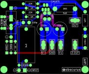
I am not keen on the L||R being on the amp PCB. I believe that is better located away from the amp. In the cable running to the output terminals.
If you remove the L||R you leave a lot of space to move the R+C VERY MUCH CLOSER to the output pin AND the power ground (PG).
The loop from output pin through the R+C to the PG, though the decoupling capacitor and back into the power pins should be kept very short and very compact to minimise interference and to minimise impedance. Minimum impedance allows the R+C to work properly at the very high frequencies that half wave stop/start have. The 100nF will span across the purple trace to reach into the middle of the power plane in between the 4 caps.
Alternatively swap the L||R with the R+C to obtain the benefits of low loop area and get the output near the edge where big stiff cable can get out easily.
Hi.
It a bit again the grounding rule what I'm follow. I current try to follow Bonsai rule which can be describe in my attatchment.
With your advice, I will have to link the R+C to the power plane in between the 4 caps which before the speaker return. Yes, I know that you want to optimize the loop area but is it have a negative affect as well if I connect the R+C before the speaker ground?
Attachments
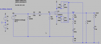
Your schema doesn't show an inductor series to V-out, but it should and here's why:
This quoted directly from the LM1875 datasheet. It was in the stability section of the official datasheet.Texas Instruments said:...couple to the load through a 10Ω resistor in parallel with a 5μH inductor
Higher value small signal ground lift resistors, such as 10R need to be bypassed by a small ceramic cap, and 100n will do for a guess. The added cap "prevents" causing a bad cap simulator, since the groundlift resistor adds to the ESR loss figure of the inverting input coupler (and by adding 10 we might get a really bad quality signal coupling cap no matter what model is purchased). This is just a tiny and not very important footnote, one that could prevent a spot of frustration later.
Obscurus, look at your sch in post707.Hi.
It a bit again the grounding rule what I'm follow. I current try to follow Bonsai rule which can be describe in my attatchment.
With your advice, I will have to link the R+C to the power plane in between the 4 caps which before the speaker return. Yes, I know that you want to optimize the loop area but is it have a negative affect as well if I connect the R+C before the speaker ground?
The route around the HF (100nF) decoupling route must be very short and very compact.
The route around the MF (100uF) decoupling can be a little longer and a bit more open (more loop area).
The route around the loop that includes the U1 output node, the R2+C1 Zobel and back to the decoupling cap junction must be short and be compact. It should be as small, or smaller, than the MF decoupling route.
All the preceding routes operate at high frequencies only. They have no purpose at audio frequencies. That is why they must have very low inductance. Low inductance comes directly from LOW LOOP AREA.
The speaker cable route is audio frequency. It is not so dependant on low inductance. It can be bigger and still work. But if you deliberately add in excessive loop area it becomes a good aerial for emitting interference. That interference can get into low level circuits and can destroy performance. Longer routes are permissible due to low frequencies but you also need lowish LOOP AREA. Keep the flow and returns very close to each other.
Now all the preceding affects the way you layout the traces on the PCB and the way you add cables out to the terminals.
Get the highest frequency parts in first and smallest.
Add on the medium frequency parts that allows access and assembly ease and keeps lowish loop area.
Finally add on the audio frequency stuff like speaker cables/traces
That should determine the locations of the parts you were asking about.
But another finally.
Low Loop Area applies to the low level input circuits as well. They form aerials. They pick up interference. Keep them very small. As small as the components themselves.
Your ultra big input capacitor could be adding more interference effects, than the benefits you gain by using the absolute best ideal capacitor. Note you have the return trace directly under the length of the capacitor. That reduces LOOP AREA. That is good.
Personally I would use a 0.2" pitch MKS/MKT/Mylar/polyester capacitor there that has an F-3dB <2Hz and gives a loop area that is propably less than 1% of what your big capacitor will result in. MKP will be bigger. FKP will be even bigger again.
Last edited:
I'm surprised Mark was able to understand what you were posting.Higher value small signal ground lift resistors, such as 10R need to be bypassed by a small ceramic cap, and 100n will do for a guess. The added cap "prevents" causing a bad cap simulator, since the groundlift resistor adds to the ESR loss figure of the inverting input coupler (and by adding 10 we might get a really bad quality signal coupling cap no matter what model is purchased). This is just a tiny and not very important footnote, one that could prevent a spot of frustration later.
I don't understand this.
Your schema doesn't show an inductor series to V-out, but it should and here's why:
This quoted directly from the LM1875 datasheet. It was in the stability section of the official datasheet.
I removed the R // L and likely will put it at the speaker connector. I also thinked you need whote the the whole text block from datasheet for better understanding.
Low Loop Area applies to the low level input circuits as well. They form aerials. They pick up interference. Keep them very small. As small as the components themselves.
Your ultra big input capacitor could be adding more interference effects, than the benefits you gain by using the absolute best ideal capacitor. Note you have the return trace directly under the length of the capacitor. That reduces LOOP AREA. That is good.
Personally I would use a 0.2" pitch MKS/MKT/Mylar/polyester capacitor there that has an F-3dB <2Hz and gives a loop area that is propably less than 1% of what your big capacitor will result in. MKP will be bigger. FKP will be even bigger again.
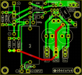
With 22K input impedance, input cap must be ~ 2.2 uf. I cant find any MKT with that value and small. I'm not sure about this, I may need some expirentment to see the affect. So bypass this ideal and will be back on it later. I come up with new layout for my LM1875. Could you have a look at it again?
Attachments
2.2 is an E3 and E6 value.
That is the most common of the value range used by capacitor manufacturers.
Rarely do we see E12, or E24, values in capacitors but there are some around.
MKS/MKT/Mylar/Polyester are almost the same. Any of these in 2u2F value would do and they are available in a 0.2" package and very cheap.
That is the most common of the value range used by capacitor manufacturers.
Rarely do we see E12, or E24, values in capacitors but there are some around.
MKS/MKT/Mylar/Polyester are almost the same. Any of these in 2u2F value would do and they are available in a 0.2" package and very cheap.
Last edited:
To your 4001, 10R, 4001 area, please add a 100n ceramic disc or "X" or SMD capacitor so you don't risk simulating a really bad cap at the 150u + 10R more ESR losses for unpleasant treble droop and lack of noise rejection performance by same factor.
Personally I would not groundlift the inverting input because only the signal area input, involving the + input has any need of the groundlift idea; however, the above note was an adequate patch, just in case you felt the need to groundlift an area not relevant to signal input ground signals.
Edit:
1k with 150u is too small, so that the diodes set parallel with the 150u will switch on and add distortion. So, please add either more capacitance or more diodes in series. We really don't want the diodes to conduct the bass! However, the circuit is excellent for proving what size (bigger) cap you should have used, albeit not so excellent for music until the cap size is increased (or other options involving lower pitched RC value, enough that the diodes don't switch on during normal music). A very educational test jig indeed!
Last edited:
To prevent treble distortion from the diode clipper positioned at inverting input, either the positive input cap has to be decreased by 6.3 times or the inverting input cap has to be increased by same factor.
If you have a subwoofer handy, choose the former, or if you want full range, choose the latter, along with 470u parallel with 470u = low loss 940u for your inverting input coupler (when series with 1k).
It is most unpleasant to apply a warmer audio effect at that particular locale (inverting input, via too small capacitor for coupler), where the costs of distortion are most severe (gain applied to distortion) and not safeguarded by a power-op-amp's distortion rejection capacity (it will obey what you put at inputs, even if you're wrong). Therefore, don't use the wrong cap size there. It would be much more fun and eventually less expensive to mod the power supply by filtering to reject noise and/or unfavorable pitches; and, other large signal components including a Padding resistor for your midrange or a BSC circuit for your 2-way speaker or full range speaker, are also, eventually, less expensive than distortion with gain applied in the amplifier. SO, don't distort the amplifier--gain applied to distortion is certainly more expensive than any size copper coil that probably isn't yet inside your speaker.
If I knew how to use LTspice I would show you the AC voltage across the DC blocking capacitor in a competently designed non-inverting amplifier.
It would be instructive to also examine the current through the protecting diode in normal operating conditions, i.e. passing an AC audio signal below clipping level.
The simulation would show you are barking up the wrong tree. I am over here
Looking at his last sch post707 we see C2=3u3F, R5=1k, R4=22k, R3=1k and C7=150uF
My usual recommendations states that C7 should be bigger than C2*(R5+R4)*sqrt(2)/R3 >3.3*(1k+22k)*1.414/1k >107uF
He has chosen 150uF. It is bigger than 107uF.
He does not need to make C7 any bigger, no matter how you say it.
Last edited:
- Home
- Amplifiers
- Chip Amps
- Beginner's Gainclone, HiFi LM1875, The Amplifier Board