Hi Mayday, I am about to start accumulating parts for the build and would appreciate some close up photos of your completed unit.
thanks
kp93300
Hi,
Two of them look like this, the third has other film caps and 6K8 resistors.
If better pics are needed, I'll take some as soon as time allows.
Attachments
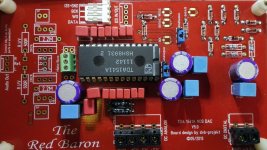
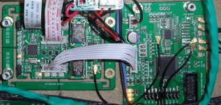
Hi Oliver,
I having troubles getting Red Baron to fly.
The signals on the le/ws, dataL and dataR TDA1541 pins are slightly above 1 V. The BCK signal is healthy 3.3V.
Before attenuation circuit all signals are 3.3 V.
Supply voltage is correct with 3.3 +-5 and -15V
Is there something wrong with my attenuation circuit?
How can I debug it?
Attachments
Hi Oliver,
I having troubles getting Red Baron to fly.
The signals on the le/ws, dataL and dataR TDA1541 pins are slightly above 1 V. The BCK signal is healthy 3.3V.
Before attenuation circuit all signals are 3.3 V.
Supply voltage is correct with 3.3 +-5 and -15V
Is there something wrong with my attenuation circuit?
How can I debug it?
View attachment 550012
View attachment 550013
View attachment 550016
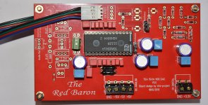
Hi,
witch Clock Modules are you using (Freq.)?
Wiring as followed:
Ian´s PCM Module --> Red Baron
LLLR --> WS/LE
CLK ---> BCK
DR ----> DATA/L
DL ----> DATA/R
Did you have sound in normal I2S mod.?
BTW, i don´t see the connection between the FIFO/Dual Clock Module and the PCM... see attached.
Best,
Oliver
Attachments
Last edited:

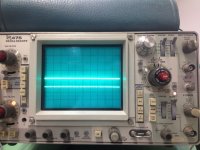
I use 45, 49 MHz clocks.
The wiring is correct, but I will check it again.
I did not try I2S yet - would be my next thing to try.
TDA1541 datasheet says 0.8 as low and 2V as high signal.
Is 1V high on TDA dataR/L pins enought?
What voltage is on your TDA dataR/L pins?
View attachment 550105
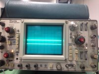
I think with 45, 49 MHz clocks, you must set th PCM board to Half-Speed mod.
Please look to Ian's thread about this.
Hi,
What is the max value of I/V resistor for onboard MOSFET buffer with +3.3V reference ground? As I understand in first step of procedure described in post #784 page 79 http://www.diyaudio.com/forums/group-buys/167414-reference-tda1541a-dac-i2s-bus-architecture-79.html#post2740927 DC offset is removed so we have +2mA to -2mA instead of 0 to -4mA signal amplitude and then the whole thing is lifted +3.3V above the GND for the sine wave never cross the zero. The upper part of sine wave is above +3.3V and the lower part is between GND and +3.3V. So the max value of the I/V resistor to stay always above GND is 3.3V / 2mA = 1650R. Is it correct?
Maciek
What is the max value of I/V resistor for onboard MOSFET buffer with +3.3V reference ground? As I understand in first step of procedure described in post #784 page 79 "Reference" TDA1541A DAC with I2S-BUS architecture DC offset is removed so we have +2mA to -2mA instead of 0 to -4mA signal amplitude and then the whole thing is lifted +3.3V above the GND for the sine wave never cross the zero. The upper part of sine wave is above +3.3V and the lower part is between GND and +3.3V. So the max value of the I/V resistor to stay always above GND is 3.3V / 2mA = 1650R. Is it correct?
There are practical limits for I/V resistor value (output impedance) in order to maintain good performance. I would not exceed 1000 Ohms.
With 4mA full scale current this translates to 4Vpp.
It is also wise to provide sufficient headroom in order to reduce distortion and prevent clipping.
If you need more, it is better to use an extra TDA1541A, this will provide 8mA combined full scale current and 8Vpp.
The MOSFET serves as grounded gate current buffer. It has low input impedance (between gate and source) and high output impedance.
Current outputs like to see a low impedance load, so voltage swing at the output is reduced to minimum. Current outputs can be short circuited to GND without damage because the Chip is designed to limit the output current to -4mA.
In order to provide a low input impedance there must be a relatively high bias current flowing through the MOSFET, even when the TDA1541A output current reaches zero.
I suggest to use -minimum- of 4mA here. There is a sweet spot like with amplifier circuits, it depends on MOSFET characteristics.
The current through the I/V resistor will then swing between -4mA and -8mA and it causes the voltage drop across the 1000 Ohm I/V resistor to vary between 4V (DAC output current equals zero), and 8V (full scale DAC output current). At digital silence the voltage drop equals 6V.
Suppose we use a 5V GND reference voltage then we need 5V (GND reference voltage) + 6V (digital silence) = 11V supply voltage for the I/V resistor. Voltage regulator of 12V would be more suitable so let’s increase the MOSFET bias current a bit.
In order to get 5V at digital silence we need 12 - 5 = 7V across the I/V resistor. This requires I = V / R = 7 / 1000 = 7mA total bias minus 2mA TDA1541A bias equals 5mA.
Bias resistor (between -15V and TDA1541A output) value equals R = V / I = 15 / .005 = 3K.
The output voltage swings symmetrically around 5V GND reference between 3V and 7V. This leaves 3V headroom at the bottom and 5V at the top ensuring low distortion.
So we end up with following circuit:
MOSFET source connects to TDA1541A output.
MOSFET drain connects to 1000 Ohms I/V resistor.
MOSFET gate connects to a trimmer. The trimmer connects between GND and +12V as we need a gate voltage that is higher than 5V !
-> Make sure the DAC is streaming digital silence! (-2mA bias).
-> trim the gate voltage for zero volts between I/V resistor output and 5V ground reference voltage (voltmeter between MOSFET drain and GND reference).
Other side of the 1000 Ohms I/V resistor connects to the +12V supply.
MOSFET bias resistor of 3K connects between -15V and the TDA1541A output.
5V GND reference voltage.
One can play around with different bias and I/V resistor values, there is plenty of headroom.
When a passive DC-coupled output is desired there is another option, although the output voltage swing will be reduced to 300mVpp and we would violate TDA1541A output compliance quite a bit.
I/V resistor for 300mVpp swing equals 0V3 / 0.004 = 75 Ohms.
Without further action the signal would swing between 0V and -0V3 and we would get a distorted signal. So we need to add exactly +150mV bias voltage.
The I/V resistor is connected to +150mV reference instead of 0V (GND). With -2mA bias current we get -0.002 * 75 = -150mV. By adding the +150mV reference voltage we get exactly zero volts at the TDA1541A output and a symmetrical swing around 0V so we can use GND as reference again.
We could construct a simple +150mV reference voltage by using a low ohmic resistive divider. For example 48R5 in series with 1.5 Ohms. Make sure the 5V supply can provide sufficient current for two channels:
5 / 25 = 200mA for both L and R channel voltage references. If this is a problem you could experiment with higher resistor values maintaining same ratio.
48.5 Ohm can be obtained by connecting a 47 Ohm and 1.5 Ohm resistor in series. Don't mix up this extra 1.5 Ohm resistor with the 1.5 Ohm resistor required for voltage division.
It could be necessary to perform some fine adjustment to get exactly zero volts DC on the TDA1541A outputs.
Circuit description:
Voltage divider, 48.5 Ohms and 1.5 Ohms in series, 1.5 Ohms connects to GND, 48.5 Ohms connects to +5V
75 Ohm I/V resistor connects between junction of 1.5 Ohms & 48.5 Ohms and TDA1541A output.
300mVpp output voltage is taken from the TDA1541A output pin.
Suitable (tube) amplifier stage can be used to obtain desired output voltage.
Other option would be using a step-up transformer:
1:3, 75 Ohms I/V, 900mVpp, 675 Ohms output impedance.
1:4, 75 Ohms I/V, 1.2Vpp, 1200 Ohms output impedance.
1:5, 75 Ohms I/V, 1.5Vpp, 1875 Ohms output impedance.
1:6, 75 Ohms I/V, 1.8Vpp, 2700 Ohms output impedance.

There are practical limits for I/V resistor value (output impedance) in order to maintain good performance. I would not exceed 1000 Ohms.
With 4mA full scale current this translates to 4Vpp.
It is also wise to provide sufficient headroom in order to reduce distortion and prevent clipping.
If you need more, it is better to use an extra TDA1541A, this will provide 8mA combined full scale current and 8Vpp.
The MOSFET serves as grounded gate current buffer. It has low input impedance (between gate and source) and high output impedance.
Current outputs like to see a low impedance load, so voltage swing at the output is reduced to minimum. Current outputs can be short circuited to GND without damage because the Chip is designed to limit the output current to -4mA.
In order to provide a low input impedance there must be a relatively high bias current flowing through the MOSFET, even when the TDA1541A output current reaches zero.
I suggest to use -minimum- of 4mA here. There is a sweet spot like with amplifier circuits, it depends on MOSFET characteristics.
The current through the I/V resistor will then swing between -4mA and -8mA and it causes the voltage drop across the 1000 Ohm I/V resistor to vary between 4V (DAC output current equals zero), and 8V (full scale DAC output current). At digital silence the voltage drop equals 6V.
Suppose we use a 5V GND reference voltage then we need 5V (GND reference voltage) + 6V (digital silence) = 11V supply voltage for the I/V resistor. Voltage regulator of 12V would be more suitable so let’s increase the MOSFET bias current a bit.
In order to get 5V at digital silence we need 12 - 5 = 7V across the I/V resistor. This requires I = V / R = 7 / 1000 = 7mA total bias minus 2mA TDA1541A bias equals 5mA.
Bias resistor (between -15V and TDA1541A output) value equals R = V / I = 15 / .005 = 3K.
The output voltage swings symmetrically around 5V GND reference between 3V and 7V. This leaves 3V headroom at the bottom and 5V at the top ensuring low distortion.
So we end up with following circuit:
MOSFET source connects to TDA1541A output.
MOSFET drain connects to 1000 Ohms I/V resistor.
MOSFET gate connects to a trimmer. The trimmer connects between GND and +12V as we need a gate voltage that is higher than 5V !
-> Make sure the DAC is streaming digital silence! (-2mA bias).
-> trim the gate voltage for zero volts between I/V resistor output and 5V ground reference voltage (voltmeter between MOSFET drain and GND reference).
Other side of the 1000 Ohms I/V resistor connects to the +12V supply.
MOSFET bias resistor of 3K connects between -15V and the TDA1541A output.
5V GND reference voltage.
One can play around with different bias and I/V resistor values, there is plenty of headroom.
Hello John,
Can you explain/described how does it all work in Olivers circuit?
The 2SK216 MOSFET bias resistor is 2.2M so the bias current is close to zero. How does it influence MOSFET input impedance?
The supply voltage for I/V resistor is 5V and is equal to 5V GND reference voltage so there is no headroom at the top.
If we decrease the GND reference to 3.3V and use 500R I/V resistor with 5V supply voltage then we have voltage swing between 2.3V and 4.3V with 2.3V headroom at the bottom and 0.7V headroom at the top.
Is it correct or I am missing something?
Regards,
Maciek
Seems I totally misunderstand the whole thing 
I've sketched the Olivers and Johns circuits in the attached pdf. Please let me know if they're OK.
Would it be safe to just change the I/V resistor in Olivers circuit to 1000R and get 4Vpp without chanching anything else?
Best regards,
Maciek
I've sketched the Olivers and Johns circuits in the attached pdf. Please let me know if they're OK.
Would it be safe to just change the I/V resistor in Olivers circuit to 1000R and get 4Vpp without chanching anything else?
Best regards,
Maciek
Attachments
I've sketched the Olivers and Johns circuits in the attached pdf. Please let me know if they're OK.
The hot side of the 250K pot in the schematic Redbaron v5.0 should be connected to +5V.
Source and drain are swapped but I assume this has been corrected by twisting the source and drain leads of the MOSFET.
Tip: When drawing schematics, draw a dot on crossing lines that need to be connected, easier to read. The 150pF needs to be connected to the 2M2 resistor so we would place a dot on these crossing lines.
Same applies for the crossing between I/V resistor and output.
The schematic I described requires no 1K potentiometer. GND reference can be connected directly to +5V.
You would have to apply following modifications to the RedBarron circuit:
- Replace 2M2 resistor with 3K resistor
- Connect GND reference to +5V, remove 470uF and 1K trimmer.
- Add a 12V regulator.
- Connect 1K to this 12V regulator.
- Disconnect the hot side (the one that is not connected to GND) of the 250K pot from the +5V and connect it to the +12V supply.
Always make sure to put a capacitance multiplier (single transistor) between rectifier and voltage regulator. Voltage regulators provide best performance when powered by a low ripple (few millivolts), slow changing input voltage.
Would it be safe to just change the I/V resistor in Olivers circuit to 1000R and get 4Vpp without chanching anything else?
Yes this should work but it’s on the edge, expect some distortion.
Source and drain are swapped but I assume this has been corrected by twisting the source and drain leads of the MOSFET.
The new Red Baron
aka TDA1541A DAC V4.0
I believe this issue was fixed in v4 of the Red Barron:
The evolution brings the following changes
- Separate I2S-GND route to Digital-GND
- Separate Analog Output GND route
- Separate GND route for active divider decoupling caps to Analog-GND
- Modified active divider decoupling pads for better SMD 1210 caps soldering
- Onboard SOT353 footprint for fastest DEM-Synchronizer IC´s
- Un-interrupted ground plane
- MOSFET Source/Drain failure corrected
So there is no need for that mod / correction.
The new Red Baron
aka TDA1541A DAC V4.0
I believe this issue was fixed in v4 of the Red Barron:
So there is no need for that mod / correction.
Correct!
The hot side of the 250K pot in the schematic Redbaron v5.0 should be connected to +5V.
Source and drain are swapped but I assume this has been corrected by twisting the source and drain leads of the MOSFET.
Tip: When drawing schematics, draw a dot on crossing lines that need to be connected, easier to read. The 150pF needs to be connected to the 2M2 resistor so we would place a dot on these crossing lines.
Same applies for the crossing between I/V resistor and output.
The schematic I described requires no 1K potentiometer. GND reference can be connected directly to +5V.
You would have to apply following modifications to the RedBarron circuit:
- Replace 2M2 resistor with 3K resistor
- Connect GND reference to +5V, remove 470uF and 1K trimmer.
- Add a 12V regulator.
- Connect 1K to this 12V regulator.
- Disconnect the hot side (the one that is not connected to GND) of the 250K pot from the +5V and connect it to the +12V supply.
Always make sure to put a capacitance multiplier (single transistor) between rectifier and voltage regulator. Voltage regulators provide best performance when powered by a low ripple (few millivolts), slow changing input voltage.
Yes this should work but it’s on the edge, expect some distortion.
Thanks for the answer John. Now evertyhing is clear
Best regards,
Maciek
Hi guys,
Need a bit of your guidance, can't figure in all hundreds of pages where can I find some guidelines for Red Baron v5.
So I've ( finally ) finished it, but the shunt regulators aren't built... so I've test it with batteries
I've turned the multiturn potentiometers for minimum DC offset on output. (~0.3V)
(seems the difference to 0V must be obtained by mounting the DC reference module o the output? ) When music plays will remain on 0V!?! No danger for headphones? Can still some couplings caps be mounted for extra safety? Sorry for being noob, but things are not so clear to me :S
PS: with some (very) cheap headpohones even in this state, the music flows from it... i'm really happy
PSS: if this is not the place to write this, I please ask a moderator to move it.
Rgs,
Alex.
Attachments
Red Baron Setting Points
Hi Alex,
here is how to use the Setting Points:
1st
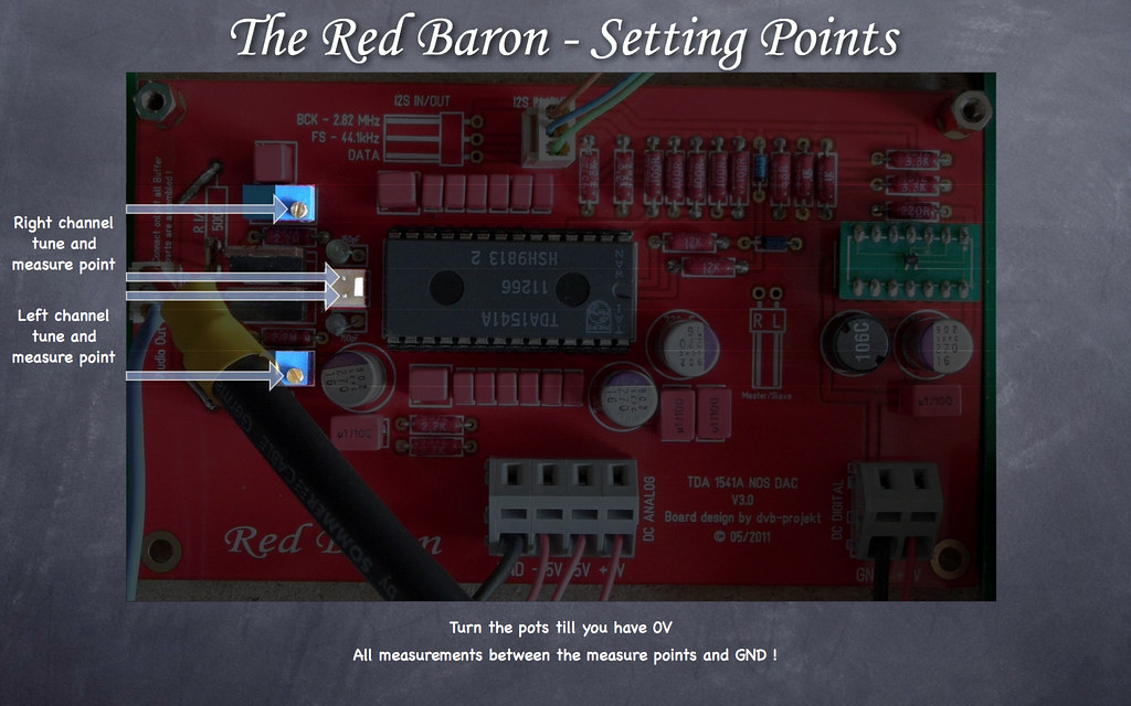
2nd
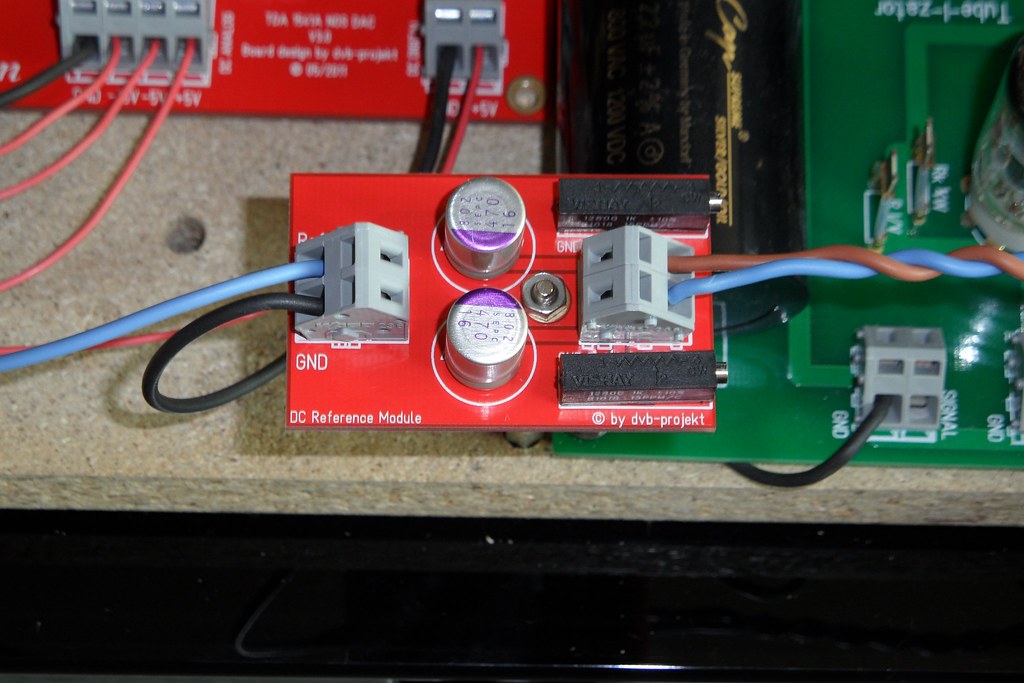
You connect the DC-Reference Module as followed:
From DAC module
Ref. (Audio out) --> Ref. +5V
GND (DC Digital) --> GND
From DC Ref. Module
GND Ref. Left --> GND RCA Left
GND Ref. Right --> GND RCA Right
Trimm the RCA GND to 0V

Hi guys,
Need a bit of your guidance, can't figure in all hundreds of pages where can I find some guidelines for Red Baron v5.
So I've ( finally ) finished it, but the shunt regulators aren't built... so I've test it with batteries
I've turned the multiturn potentiometers for minimum DC offset on output. (~0.3V)
(seems the difference to 0V must be obtained by mounting the DC reference module o the output? ) When music plays will remain on 0V!?! No danger for headphones? Can still some couplings caps be mounted for extra safety? Sorry for being noob, but things are not so clear to me :S
PS: with some (very) cheap headpohones even in this state, the music flows from it... i'm really happy
PSS: if this is not the place to write this, I please ask a moderator to move it.
Rgs,
Alex.
Hi Alex,
here is how to use the Setting Points:
1st
2nd
You connect the DC-Reference Module as followed:
From DAC module
Ref. (Audio out) --> Ref. +5V
GND (DC Digital) --> GND
From DC Ref. Module
GND Ref. Left --> GND RCA Left
GND Ref. Right --> GND RCA Right
Trimm the RCA GND to 0V
- Status
- This old topic is closed. If you want to reopen this topic, contact a moderator using the "Report Post" button.
- Home
- Group Buys
- "Reference" TDA1541A DAC with I2S-BUS architecture