Hello everyone!
I´m designing a new guitar amplifier with a fet gain stage. By now I´m using MMBF5457.
But I´m getting a wierd distortion out of it. It´s not a harmonic distortion. By listeting to it, my first thought were that there was something loose in the speaker cabinet, something metal part ringing. But even changing the cabinet, the same noise appeard...
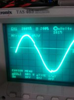
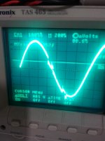
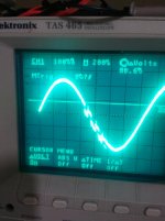
After long hours analysing the circuit I finally could find and see this distortion on the osciloscope. It looks like some kind of crossover distortion.
I never found anything like this, and I have no idea of how resolve this...
I´ve tried to chage the fet but still no sucess...
I´m uploading some pics os the osciloscope, for diferent signal amplitudes just after the FET stage.
It´s an ordinary commun sorce gain stage.
Any hints on how to solve this??
Thanks a lot guys!
I´m designing a new guitar amplifier with a fet gain stage. By now I´m using MMBF5457.
But I´m getting a wierd distortion out of it. It´s not a harmonic distortion. By listeting to it, my first thought were that there was something loose in the speaker cabinet, something metal part ringing. But even changing the cabinet, the same noise appeard...
After long hours analysing the circuit I finally could find and see this distortion on the osciloscope. It looks like some kind of crossover distortion.
I never found anything like this, and I have no idea of how resolve this...
I´ve tried to chage the fet but still no sucess...
I´m uploading some pics os the osciloscope, for diferent signal amplitudes just after the FET stage.
It´s an ordinary commun sorce gain stage.
Any hints on how to solve this??
Thanks a lot guys!
Attachments
Looks like something's breaking into oscillation (at a higher freq than your scope can see). Without a schematic I can't guess what parts though. If it's the FET try putting a few hundred pF from drain to gate, see if that fixes. Could be a different stage though. If there are power MOSFETS around, be sure to add about 1k ohm in series on their gates.
Hi there!
Well, thank you for the comments!
Tomorow I will try some capacitor between drain and gate and see what happens.
Acutually, I dont think it's oscilation becuse that happens only with a short range input signal amplitude. There is no noise/ditortion with low amplitude signals nor with larger noises, just before the fet breaks into cutoff, what is intended in this case.
But I'm just getting into jfet stuff, so any hint will help a lot.
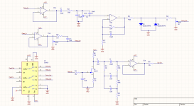
My schematic was on multiple sheets, so I rearranged to show fet surroundings.
Basicaly the jfet is driven by a CMOS switch, a CD4053. Althoug I tried once to bypass the switch and the problem persisted. (By bypassing the switch, a Op Amp drove the fet).
Well, thank you for the comments!
Tomorow I will try some capacitor between drain and gate and see what happens.
Acutually, I dont think it's oscilation becuse that happens only with a short range input signal amplitude. There is no noise/ditortion with low amplitude signals nor with larger noises, just before the fet breaks into cutoff, what is intended in this case.
But I'm just getting into jfet stuff, so any hint will help a lot.
My schematic was on multiple sheets, so I rearranged to show fet surroundings.
Basicaly the jfet is driven by a CMOS switch, a CD4053. Althoug I tried once to bypass the switch and the problem persisted. (By bypassing the switch, a Op Amp drove the fet).
Attachments
Hello again!
I´v just insert a 220pF between drain and gate. Indeed distortion/oscilation has reduced.
Than I´v tried raise it to 440pF, and it got even better. But I still can hear it...
It seens that now the oscilation only comes with higher input sinals.
I can keep raising this capacitance, but there must be another way to solve this
Actually the CMOS switch is driving the jfet.
And I´m quite sure that the oscilation is coming from the jfet...
Those pics I sent were right from jfets drain.
And a clear signal was seen at jfets gate
I did that to cut highs at jfets input.
I´v just insert a 220pF between drain and gate. Indeed distortion/oscilation has reduced.
Than I´v tried raise it to 440pF, and it got even better. But I still can hear it...
It seens that now the oscilation only comes with higher input sinals.
I can keep raising this capacitance, but there must be another way to solve this
It looks like what we call a parasitic oscillation, rather than a constant oscillation.
So the op amp drives the JFET? Is this distortion on the output pin of that op amp?
Actually the CMOS switch is driving the jfet.
And I´m quite sure that the oscilation is coming from the jfet...
Those pics I sent were right from jfets drain.
And a clear signal was seen at jfets gate
Why is there a large capacitor from the gate to ground?
I did that to cut highs at jfets input.
Last edited:
And I´m quite sure that the oscilation is coming from the jfet...
Those pics I sent were right from jfets drain
That doesn't mean it is caused by it.
Jan
To me the plot looks like a sine wave with a small added square wave.
I would check for any crosstalk from other parts of the circuitry.
Is your drive channel driven instantaneously with input signal?
In that case its output delivers a square wave and crosstalk is plausible.
I would check for any crosstalk from other parts of the circuitry.
Is your drive channel driven instantaneously with input signal?
In that case its output delivers a square wave and crosstalk is plausible.
That doesn't mean it is caused by it.
Jan
Sory Jan,
I edited my post while you posted
I have a clean signal at jfets gate.
Thats why I sticked with the jget distortion/oscillation hypotesis.
Althoug I started thinking about some coupling problems.
I´ve been reading abou parasitic oscillation and well... it really looks what I got here...
I´m quite sure that I have a bad pcb design problem here...
I didnt know fets where so susceptible to parasitic oscillation...
I have a quite long track from the CMOS switch and the jfet. And by inserting a wire parallel to this track the oscillation raised.
By now I will filter as much as I can and soon I will design a new pcb
Since you are at it, I also see some other questionable points in your design you might want to correct:
1) you already mentioned it, the long track feeding the FET gate, which is a very high impedance sensitive point.
2) you have no ground reference for that gate
When CMOS switch opens to go to the other channel, it's left floating and undefined.
Add a 1M resistor gate to ground.
3) 10k+2n2 is a steep HF cutoff, if you *need* it (and it still doesn't fully work) it means you still have *other* uncorrected problems.
To be more precise: 10k+2n2 is around 8kHz and seems to be above guitar frequencies ... but that only if said 2n2 capacitor is driven from a low impedance, say a nearby Op Amp or a signal generator output, but if driven from, say, a tone control or a volume pot or mixing resistor, then those 2n2 become an important load.
Which ones? not sure, don't have your amp on my bench to test, but would suspect poor grounding and (again) poor layout.
Not dissing you at all (fica tranqüilo irmão") ) but PCB layout is some sort of black art , even more so in high gain low signal high impedance circuits, takes years of experience to get well the most complex ones.
) but PCB layout is some sort of black art , even more so in high gain low signal high impedance circuits, takes years of experience to get well the most complex ones.
As a side note, forget autorouters, put tracks where YOU want, by hand.
4) why do you work at such low impedance levels?
You seem to have chosen 1k pots all over the place (why? was it some starting generic value in the simulator software?).
Not very common to begin with and definitely not available over the counter (specially in Brazil) in Audio/Log taper, what you need for volume and distortion drive.
5) you added a fixed tone control after vthe FET, á la JCM900 .
top right C2+R14 is fine, those are common values for the Treble control, but left bottom R13+C5 are plain wrong.
To begin with crossover frequency is around 1500 Hz, WAY too high for a BASS control, and to boot, around 10k impedance is very poorly driven (that's an understatement) from 5X higher impedance at Tr1 drain (47k) .
Typical values are 100k to 33k and 47nF to 22nF .
6) your clean channel bright pot, C11 will have little to no effect, since it's used with a 1k pot but has 2k2 in series.
We are talking around 1dB treble boost here, pretty unnoticeable.
In any case, I suggest you Protoboard your designs first, tweak as needed until you find a sound you like, and only after that you commit to a PCB.
It might also help to study a few commercially succesful designs to see how they did things.
1) you already mentioned it, the long track feeding the FET gate, which is a very high impedance sensitive point.
2) you have no ground reference for that gate
When CMOS switch opens to go to the other channel, it's left floating and undefined.
Add a 1M resistor gate to ground.
3) 10k+2n2 is a steep HF cutoff, if you *need* it (and it still doesn't fully work) it means you still have *other* uncorrected problems.
To be more precise: 10k+2n2 is around 8kHz and seems to be above guitar frequencies ... but that only if said 2n2 capacitor is driven from a low impedance, say a nearby Op Amp or a signal generator output, but if driven from, say, a tone control or a volume pot or mixing resistor, then those 2n2 become an important load.
Which ones? not sure, don't have your amp on my bench to test, but would suspect poor grounding and (again) poor layout.
Not dissing you at all (fica tranqüilo irmão
) but PCB layout is some sort of black art , even more so in high gain low signal high impedance circuits, takes years of experience to get well the most complex ones.As a side note, forget autorouters, put tracks where YOU want, by hand.
4) why do you work at such low impedance levels?
You seem to have chosen 1k pots all over the place (why? was it some starting generic value in the simulator software?).
Not very common to begin with and definitely not available over the counter (specially in Brazil) in Audio/Log taper, what you need for volume and distortion drive.
5) you added a fixed tone control after vthe FET, á la JCM900 .
top right C2+R14 is fine, those are common values for the Treble control, but left bottom R13+C5 are plain wrong.
To begin with crossover frequency is around 1500 Hz, WAY too high for a BASS control, and to boot, around 10k impedance is very poorly driven (that's an understatement) from 5X higher impedance at Tr1 drain (47k) .
Typical values are 100k to 33k and 47nF to 22nF .
6) your clean channel bright pot, C11 will have little to no effect, since it's used with a 1k pot but has 2k2 in series.
We are talking around 1dB treble boost here, pretty unnoticeable.
In any case, I suggest you Protoboard your designs first, tweak as needed until you find a sound you like, and only after that you commit to a PCB.
It might also help to study a few commercially succesful designs to see how they did things.
Get rid of the input capacitor. It combined with the layout inductance is a classic oscillator when the input signal biases the FET into operating range. If you want a low pass either place it in a feedback loop or insert a resistor of 1000 ohms in series with the capacitor.
JMFahey, my first look at the schem and also saw no resistor from Jfet gate to ground(!) so agreed point 2 very good place to correct that first, isolate the solid state switches. get the stage working right then add the SS switches etc. I did some Fet preamps with 2 and 3 stages, and those circuits like high value resistive controls, 500K and 1 Meg pots. They are still quite quiet. Biasing one stage to hit cutoff no problem, you get some nice crunch. Of course all other points all of you suggest are excellent as usual!
Thank you guys!
This afternon I´ll try some of those tips!
Those were really interesting comments!
Thanks a lot for those comments Fahey!
2) Indeed... that was a big mistake I totally forgot!
3) At first I wanted to simulate tubes miller capacitance and grid stopper resistors... But now I realise it was made in a bad way...
(BTW, I have access to some really interesting routing softwares, mainlly one called TopoRouter, a really nice topological rounter. For those complex projects I route by hand indeed.
I do want to get to know more about PCB design for audio. I only have materials on high speed digital design. The basis might be the same, but differs a lot on the pratical way)
4) Well, I do have easy access to 1k pots.
Actually I work with electronics (mailly digital). So with my background I have a tendency to go low inpedance to avoid interference. Probably I´m doing it wrong here....
5) Ops... I´ve realised I sent you guys some old version with bad values on it...
R13 is actually 100k, C5 is 33nF and R17 is 68k
6) R28 and C11 were on a kind of generic starting point values, for some fine tune later on the PCB.
Indeed I changed R28 for a jumper.
This afternon I´ll try some of those tips!
Those were really interesting comments!
Since you are at it, I also see some other questionable points in your design you might want to correct:
1) you already mentioned it, the long track feeding the FET gate, which is a very high impedance sensitive point.
2) you have no ground reference for that gate
When CMOS switch opens to go to the other channel, it's left floating and undefined.
Add a 1M resistor gate to ground.
3) 10k+2n2 is a steep HF cutoff, if you *need* it (and it still doesn't fully work) it means you still have *other* uncorrected problems.
To be more precise: 10k+2n2 is around 8kHz and seems to be above guitar frequencies ... but that only if said 2n2 capacitor is driven from a low impedance, say a nearby Op Amp or a signal generator output, but if driven from, say, a tone control or a volume pot or mixing resistor, then those 2n2 become an important load.
Which ones? not sure, don't have your amp on my bench to test, but would suspect poor grounding and (again) poor layout.
Not dissing you at all (fica tranqüilo irmão
As a side note, forget autorouters, put tracks where YOU want, by hand.
4) why do you work at such low impedance levels?
You seem to have chosen 1k pots all over the place (why? was it some starting generic value in the simulator software?).
Not very common to begin with and definitely not available over the counter (specially in Brazil) in Audio/Log taper, what you need for volume and distortion drive.
5) you added a fixed tone control after vthe FET, á la JCM900 .
top right C2+R14 is fine, those are common values for the Treble control, but left bottom R13+C5 are plain wrong.
To begin with crossover frequency is around 1500 Hz, WAY too high for a BASS control, and to boot, around 10k impedance is very poorly driven (that's an understatement) from 5X higher impedance at Tr1 drain (47k) .
Typical values are 100k to 33k and 47nF to 22nF .
6) your clean channel bright pot, C11 will have little to no effect, since it's used with a 1k pot but has 2k2 in series.
We are talking around 1dB treble boost here, pretty unnoticeable.
In any case, I suggest you Protoboard your designs first, tweak as needed until you find a sound you like, and only after that you commit to a PCB.
It might also help to study a few commercially succesful designs to see how they did things.
Thanks a lot for those comments Fahey!
2) Indeed... that was a big mistake I totally forgot!
3) At first I wanted to simulate tubes miller capacitance and grid stopper resistors... But now I realise it was made in a bad way...
(BTW, I have access to some really interesting routing softwares, mainlly one called TopoRouter, a really nice topological rounter. For those complex projects I route by hand indeed.
I do want to get to know more about PCB design for audio. I only have materials on high speed digital design. The basis might be the same, but differs a lot on the pratical way)
4) Well, I do have easy access to 1k pots.
Actually I work with electronics (mailly digital). So with my background I have a tendency to go low inpedance to avoid interference. Probably I´m doing it wrong here....
5) Ops... I´ve realised I sent you guys some old version with bad values on it...
R13 is actually 100k, C5 is 33nF and R17 is 68k
6) R28 and C11 were on a kind of generic starting point values, for some fine tune later on the PCB.
Indeed I changed R28 for a jumper.
- Status
- This old topic is closed. If you want to reopen this topic, contact a moderator using the "Report Post" button.
- Home
- Live Sound
- Instruments and Amps
- FET wierd unharmonic distortion