I finished reading the 2 books from Cordell and Self lately, will need to re-read both a couple more times, but I think it'll strengthen my understanding by an actual practice, so here I am with my first attempt to design an amplifier.
I have an IT background so I'm fairly technical, but I knew very little about electronics when I started this DIY hobby a year ago, so many of these things are entirely new for me. Hence, it's quite probable that I made a few mistakes somewhere, so your comments, corrections and suggestions are really welcomed.
Thanks and regards.
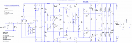
- It's a classical LIN type of topology, naturally as that's what the 2 books are about;
- I want to try something slightly different from a standard Blameless, so I've taken a push-pull VAS published by Samuel Groner couple years back, and bundle it with a EF3 from Cordell's book;
- Target: 100W into 8R, 200W into 4R, 26dB close loop gain, simulated performance similar to a typical Blameless;
- I hope it'll end up as something useful in my living room and sounding alright, instead of a giant oscillator busted into flames, so I've targeted conservative phase margin and gain margin. I also included VI limiting for more protection.
- THD1K@8R: 10.2ppm@1W, 10.1ppm@10W, 10.0ppm@100W
- THD20K@8R: 9.7ppm@1W, 23.9ppm@10W, 16.0ppm@100W
- THD1K@4R: 10.1ppm@1W, 9.9ppm@10W, 9.6ppm@100W, 10.0ppm@200W
- THD20K@4R: 31.4ppm@1W, 40.0ppm@10W, 33.1ppm@100W, 46.7ppm@200W
I have an IT background so I'm fairly technical, but I knew very little about electronics when I started this DIY hobby a year ago, so many of these things are entirely new for me. Hence, it's quite probable that I made a few mistakes somewhere, so your comments, corrections and suggestions are really welcomed.
Thanks and regards.
Attachments
-
 My_Amp 0.4b.PNG256.1 KB · Views: 859
 -
My_Amp.zip7.7 KB · Views: 93
-
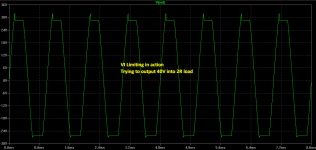 VI Limiting 40V into 2R.PNG28.4 KB · Views: 152
 -
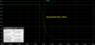 Slew Down (with input network).PNG35.5 KB · Views: 136
 -
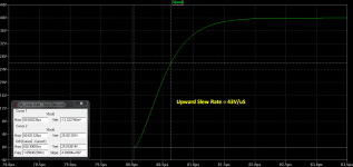 Slew Up (with input network).PNG35.1 KB · Views: 126
 -
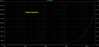 Output Impedance.PNG22 KB · Views: 138
 -
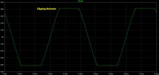 Clipping.PNG16.6 KB · Views: 641
 -
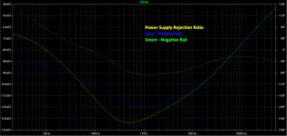 PSRR.PNG34.1 KB · Views: 671
 -
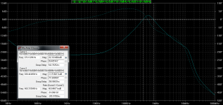
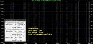 Loop Gain.PNG66.9 KB · Views: 704
 -
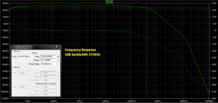 Frequency Response.PNG53.8 KB · Views: 804
Hi Guys
Some really nice plots there.
In practice, the 1uF supply bypass should be increased a thousand-fold, a bypass should be added for the output stage, and the zeners should have caps across them for the input stage. Zeners tend to be noisy.
The 100uF cap in the feedback loop is way undersized. It is contributing significant THD to all numbers. Same with the input cap. usually for simulation, those caps are left out to be able to assess what the active part of the circuit is doing. There has been enough independent study made about capacitors to kiow the range of values and dielectric types to use in the various circuit points. For example, an electrolytic is fine in the feedback network provided it is not used to shape the low-frequency response, i.e.e it should be several millifarads. The input cap should be polypropylene not polyester, as the latter introduces significant third-harmonic THD where PP does not.
You should try a sim using a standard up to date Lin-Thompson front endjust for reference. It is pedestrian but exhibits very good performance. When I first started learning to use LTspice, the Lin gave best performance but my favourite circuits are fully symmetrical. I now have the latter outperforming the Lin. I'm sure you will achieve the same end with your circuit with a little persistence.
Have fun
cwtim,
Good on you for jumping in and having a go.
You wanted to get away from the standard blameless, well you certainly have. There is little of the concepts of blameless in there. Notably simplicity, which is where I become rather uncomfortable on your behalf.
Can I suggest that as an alternative to simulation you turn your hand to a bit of prototyping and building. I expect you will learn a couple of very important lessons:
-1- In simplicity is beauty
-2- In a feedback amplifier stability is overwhelmingly important, and controlling this is best managed through simplicity (refer 1.)
-3- It is possible to hack into a cad package something that is awesomely complex, but actually works worse in the real world than much simpler approaches (refer 1)
-4- Achieving ppm level THD is not easy in reality - though simulators will make all manner of promises. Build a prototype and measure the THD - the measurements alone I promise will challenge you.
(OPINION WARNING HERE: I challenge you to hear the difference between 1 and 10ppm, probably 100ppm and maybe even 1000 in some cases).
I have seen plenty of people showing simulations of sub PPM designs. Actualising these in the real world is a completely different kettle of fish:
- Many of these rely on insane levels of loop gain and bags of feedback.
- Physical layout, power and grounding issues etc can easily swamp this - I have seen simple wiring layout add 10 times this
- measuring this is really (really!) hard in the real world
What is my point?
If this is your first effort, the place for you to start is being able to design something that just works. If you start with such a complex, and in my mind potentially marginal, design it will be really frustrating.
Don't let silly numbers and idealistic goals of "zero" distortion and suchlike distract you from the essential need for a stable, manufacturable design that won't burst into seven sorts of instability and fry your speakers.
Build something and feel the pleasure at seeing it work. You will quickly realise that you don't need to have dome something massively complicated to achieve that outcome. Indeed.... in simplicity is beauty.
... You should try a sim using a standard up to date Lin-Thompson front endjust for reference...
Thanks Struth, I’ll try your suggestions, I Googled a bit but don’t managed to find the Lin-Thompson front end you referred, could you share with me the relevant schematic or send me a link.
Thanks googlyone, all wise words and I actually agree with most (if not all) of what you said.
I also like simplicity, the only amplifier I actually built (designed by a forum member) has 4 transistors on each channel, and it’s indeed satisfying to listen to it, but it’s a bit low on the power department (10W Class A). I then acquired the parts to build a Pass F6, but a F6 still quite doesn’t give the power to drive the 4R speakers that I want to drive, so I turned to try designing one.
I did prototype, I put one channel of Blameless (OPS just 2 TO-92 transistors) on a breadboard and it worked, I also put one channel of the above VAS on a breadboard (again TO-92 OPS) and it oscillated at 26MHz, only cured by adding C12/13. What’s interesting was that such oscillation was predicted by a gain peaking at the same frequency in LTSpice. I understand the limitation of simulations, it can give all sort of wrong predictions, but it can still be useful if the right questions are asked and interpreted correctly – though admittedly I’m still learning how to do that.
Not disagreeing, but could you elaborate this point – I thought I’m playing safe by the gain and phase margin figures, and I gave up the more advanced compensations because of stability concerns – so I definitely want your further input here.
I also like simplicity, the only amplifier I actually built (designed by a forum member) has 4 transistors on each channel, and it’s indeed satisfying to listen to it, but it’s a bit low on the power department (10W Class A). I then acquired the parts to build a Pass F6, but a F6 still quite doesn’t give the power to drive the 4R speakers that I want to drive, so I turned to try designing one.
I did prototype, I put one channel of Blameless (OPS just 2 TO-92 transistors) on a breadboard and it worked, I also put one channel of the above VAS on a breadboard (again TO-92 OPS) and it oscillated at 26MHz, only cured by adding C12/13. What’s interesting was that such oscillation was predicted by a gain peaking at the same frequency in LTSpice. I understand the limitation of simulations, it can give all sort of wrong predictions, but it can still be useful if the right questions are asked and interpreted correctly – though admittedly I’m still learning how to do that.
... If you start with such a complex, and in my mind potentially marginal, design it will be really frustrating ...
Not disagreeing, but could you elaborate this point – I thought I’m playing safe by the gain and phase margin figures, and I gave up the more advanced compensations because of stability concerns – so I definitely want your further input here.
... but could you elaborate this point –
I am very much of the same opinion so if I may comment.
Most of the ultra low distortion simulations are very suspect so I would not be too disappointed if your amp does not reach that level.
But if the objective is only, say 10 ppm then you don't need that much complexity.
To be more specific, you have a second section composed of an EF assisted VAS plus folded cascodes. That's a complex loop to wrap compensation around.
You should place a Tian probe within this loop to check stability.
There's more to stability than the one loop you have checked
")
Also the push/pull schemes are vulnerable to surprises if the two sides do not match perfectly.
Very easy to miss this in simulation, since the values will all be perfect.
You need to check this manually in LTSpice, try the effect of imperfect matches for transistors and especially Miller capacitors.
Bob Cordell touches upon this but does not emphasize it, he often uses other methods to avoid the problem.
Best wishes
David
I had the comments about the inner loop stability more or less written before you posted on the 26 MHz instability.
Should have replied quicker so I could prove it wasn't just "wise after the event".
You will need also to check stability as the amp approaches the rails, with an OPS, in both simulation and reality.
This has a major effect, as do difficult loads so they need checks too.
Last edited:
Hi Guys
Everyone calls what Self names the 'blameless' a Lin, which is incorrect. The Lin circuit is just a unity-gain output stage preceded by a voltage gain stage, so the last two-thirds of the blameless. I believe it was Wahab who pointed out that it was Thompson who added the diff amp in front of the Lin to create the ubiquitous circuit that is 99% of all amps produced.
I believe going after the lowest THD possible is a must if you want a transparent circuit. There are natural distortions of sounds we hear but those generated in electronics are quite a different thing and need to be minimised as much as possible. No one can tell you how accurate spice will be compared to the real circuit, since there are too many variables and too many assumptions built into both the models and the sim algorithms. Simpler circuits seem to sim faster and real measurements corroborate performance. More complex circuits take longer to sim and tend to deviate more from the real world.
Were you to assume that the sim is off by an order of magnitude being too optimistic, then a 100ppb becomes 1ppm, which is below the resolution of an Audio precision system. This fact does not make the distortion inaudible. It is incredible what our ear is sensitive to. You will be thrilled to have a working circuit with 10% THD but it will quickly lose its luster once you live with it for a little while, especially if you listen to music that is "busy" in the midrange. The guys who like those single-mosfet amps and other similar circuits tend to listen to rather spacious music. I found the JLH to sound dreadful with any kind of modern music, but low-THD amps sound much better. Everyone has their own take on this.
As the poster above said, wiring and layout errors easily swamp the inherent performance of the circuit. Generally, if the board is laid out as the schematic is drawn, assuming a properly drawn schematic as your are, then the performance of the circuit will be pretty good. A convoluted signal path guarantees instability.
You might find the THD is lower if you take out the middle part of the circuit and use a conventional bias circuit driven by the VAS. This will allow optimisation of the idle condition for lowest THD. The current sources used are not the best ones - the feedback type is more linear. Personally, I am not a fan of circuits where the audio signal is holding off the output stage, as here. Pull-up/down is limited by the current source. Signal-driven pull-up/down provides as much drive as is needed for any load and any device set.
Have fun
... That's a complex loop to wrap compensation around ...
Thanks David for your various remarks, very useful. I'll check this loop, it's not immediate obvious to how me on how to check the inner loop stability, but I'll do my homework to try to figure out first. (As I said many of these are new to me - it took me a good night of Google searches to learn how to plot loop gain with the Tian probe in it's basic form, and I still haven't figure out how to use a GFT probe). I might come back with a question in case I'm stuck.
From an engineering perspective, this VAS is probably unnecessarily complex for what I'm trying to do, but I selected this VAS cause I think it'll lead to more learning than a standard Blameless architecture, from this perspective it's probably a good choice ... another VAS I considered is the SuperTIS, but it's way too advance for me and I might try that when there is more knowledge under my belt.
...Have fun
Thanks again, I think I'll be busy in the next few weeks to try out the various suggestions
...I'll check this loop, it's not immediate obvious to me on how to check the inner loop stability...
Or to most people
Two factors for this.For a simple Miller compensated amp the inner loop is usually stable, so there are usually no problems even if full checks are not done.
So most people are a bit careless but you should not be if you want to try less conventional circuits.
Secondly, a push/pull amp is more difficult to check stability in the inner loop.
Requires a balun, I posted one in the tread about Paul's "lunch-break" amplifier.
You are welcome to copy it and use.
Dr P J Hurst has a nice article about this on the Web, recommended for a technically minded person like you.
Best wishes
David
I believe it was Wahab who pointed out that it was Thompson who added the diff amp in front of the Lin to create the ubiquitous circuit that is 99% of all amps produced.
I recall that it was actually Michael Kiwanka.
He was criticised as a pedantic quibbler but seems to be correct on this one so it's only fair to cite him.
Last edited:
Or to most people
Hi David,
I'll second that. I had a nightmare getting my head around the placement of the probes. Persistence is key.
Secondly, a push/pull amp is more difficult to check stability in the inner loop.
Requires a balun, I posted one in the tread about Paul's "lunch-break" amplifier.
You are welcome to copy it and use.
Best wishes
David
Thought I'd add a link to an .asc with your tools for cwtim01...
http://www.diyaudio.com/forums/solid-state/265449-amp-designed-during-lunch-breaks-2.html#post4142141
This is an interesting thread. It uses a toplogy I have never even considered. So hopefully will learn something and maybe even be able to contribute something useful.
Paul
P.S. The lunch break project is still progressing. Just slowly.
I finished reading the 2 books from Cordell and Self lately, will need to re-read both a couple more times, but I think it'll strengthen my understanding by an actual practice, so here I am with my first attempt to design an amplifier.
Attached are the schematic and some simulation results. In terms of simulated THD, figures are:
- It's a classical LIN type of topology, naturally as that's what the 2 books are about;
- I want to try something slightly different from a standard Blameless, so I've taken a push-pull VAS published by Samuel Groner couple years back, and bundle it with a EF3 from Cordell's book;
- Target: 100W into 8R, 200W into 4R, 26dB close loop gain, simulated performance similar to a typical Blameless;
- I hope it'll end up as something useful in my living room and sounding alright, instead of a giant oscillator busted into flames, so I've targeted conservative phase margin and gain margin. I also included VI limiting for more protection.
I believe these THD numbers are OK but not great, especially when sub-ppm designs are widely available in this forum. I was excited by some ppb level THD1K numbers with the circuit at some stage, but when I added safety features like zobels at the OPS transistors, base stoppers, feedback DC blocking capacitor ... etc, the THD degraded to the above at the end. I tried to mess with TPC, TMC and OIC to improve the performance, but trial and error didn't get me very far and I ended up sticking with Cdom compensation. Anyway, my novice construction skill will be the limiting factor of any actual build, so I decided to settle with these THD figures for now.
- THD1K@8R: 10.2ppm@1W, 10.1ppm@10W, 10.0ppm@100W
- THD20K@8R: 9.7ppm@1W, 23.9ppm@10W, 16.0ppm@100W
- THD1K@4R: 10.1ppm@1W, 9.9ppm@10W, 9.6ppm@100W, 10.0ppm@200W
- THD20K@4R: 31.4ppm@1W, 40.0ppm@10W, 33.1ppm@100W, 46.7ppm@200W
I have an IT background so I'm fairly technical, but I knew very little about electronics when I started this DIY hobby a year ago, so many of these things are entirely new for me. Hence, it's quite probable that I made a few mistakes somewhere, so your comments, corrections and suggestions are really welcomed.
Thanks and regards.
Hello and enjoy your New project undertaking.. Just to add care is needed when working with psu voltages and currents as being zapped from them is painful..a 60w bulb is handy for draining that away..Its also a good ideal to Check units once built with no loads, transistor amps are fine to Power on unlike valve units that need loads..
You might incounter dc on the amps o/p put this a commom problem of small transistors connected in the worng way. .Most of us here have been in the Electronics Service trade for years and Seen many many amplifiers...
Remember amplifiers under Test can work on lowered supply rails so a amplifier that says 70v +/- is ok to Power on with Test voltage of 30 +/- to See if things See ok...anyway best of luck there..
Kind regards.
A.
Just a few notes so I don't have to remember them for next time.
Samuel (and you) have the current mirror capacitors C1 and C2 equal.
This is such an obvious choice that it is easy to miss that is a choice.
But I tried this in a conventional current mirror loaded LTP and found I could do better with non equal values.
When you think about it, the two transistors are connected quite differently so it's not actually obvious that equal values are best.
Not sure it's applicable here but worth a check.
Your bias spreader is a CFP, these are notorious for local loop instability.
Probably not worth the risk for a first build (and possibly not ever).
I recommend an impedance compensation resistor as discussed in Self and Cordell. Should have most of the benefits of your CFP and practically no down side.
The capacitors C4 and C5 are described by Samuel as feed forward compensation.
I have never analysed this feed-forward but I suspect it's like so called "Transitional Miller Compensation", both in the essential mechanism and also in the fact that the intuitive explanation can rather mislead.
So, careful simulation is called for in this loop I think.
Best wishes
David
@Paul
Nice to read the lunch break amp proceeds.
I have started to think about the front end layout too, I look forward to see yours.
Last edited:
...You are welcome to copy it and use...Dr P J Hurst has a nice article about this...
Thanks again. Is "Determination of stability using return ratio..." the article you're referring to? Just downloaded it, it'll be a great challenge for me to understand it though
... Thought I'd add a link to an .asc with your tools for cwtim01...
Thanks Paul, I also follow your thread about the lunch amp, I wish I could have such long lunches also, and it would be great to have your comments and ideas.
... careful simulation is called for in this loop I think ...
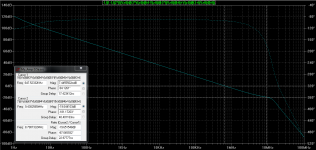
Without understanding how it works, I've taken the probe from Paul's file and insert the probe at similar positions. Got the attached result - doesn't seem right to me, so need to experiment more with it.
Attachments
Last edited:
Hello and enjoy your New project undertaking...
Thanks amptech for you good advices.
I still remember the explosion when I reversed the polarity of a 1500uF cap a year ago, and have been very careful since then when dealing with voltages and currents .
Thanks Paul, I also follow your thread about the lunch amp, I wish I could have such long lunches also, and it would be great to have your comments and ideas.
Thank you for following my mad little project.
These days the lunches are not that long. They found out I could design something... Now they've got me doing inverter design...
Without understanding how it works, I've taken the probe from Paul's file and insert the probe at similar positions. Got the attached result - doesn't seem right to me, so need to experiment more with it.
You need to remove the AC source at the front end of your amp. This interferes with the tian probe. The plots look much nicer once this has been removed.
Need to have a think about the probe placement... It's all still relatively new to me and thinking takes a long time.
Paul
Last edited:
Yes....Is "Determination of stability..." the article...?
...I've taken the probe from Paul's file and insert the probe at similar positions...
Position looks correct - as Paul noted, need to turn off the input V source.
Post the Include file of models and we can try it too.
Best wishes
David
Post the Include file of models and we can try it too.
Best wishes
David
Or better still, would it be possible to add the model definitions to the .asc file as an spice operative? That way we can just hit the start sim button.
Paul
... would it be possible to add the model definitions to the .asc file as an spice operative? ...
Certainly
, attached. I removed the AC source and the plot looks more reasonable now, at the same time it looks remarkably similar to the outer loop, need to think about what that means Attachments
- Status
- This old topic is closed. If you want to reopen this topic, contact a moderator using the "Report Post" button.
- Home
- Amplifiers
- Solid State
- My First Amplifier Design