I made a graph to show how degeneration affects thermal stability. It works for any package, insulator, heatsink, voltage, current, Re or Vdegen scenario. You'll have to look at it a bit to figure out how to use it. The thermal resistance you get from this chart is the minimum stable value for Rjh (junction to heatsink), or if you are not using thermal compensation, Rja (junction to room/ambient temp). It is based on the threshold of instability for the thermal circuit. And it may be wrong so it would be nice if someone would check it.
The result given by this chart is the absolute minimum for stability. Even if it's stable, circuits close to the threshold will experience significant thermal drift during operation. So the margin should not be just +20% for instance, but rather a multiple of five or so depending on how much drift is acceptable while the thermal compensation is catching up, and that may be the subject for another chart).
There are exceptions to this behavior. One is an EF stage without paralleled outputs and a Vbe multiplier feedback loop. The Vbe multiplier cancels the tempco of the output bias. However within the feedback delay window, the crossover bias will experience more fluctuation if there is less degeneration. Transistors with built-in thermal diodes for compensation are ideal for this since they reduce the thermal feedback lag.
When temperature feedback such as a thermally coupled Vbe multiplier is used, overall thermal runaway is usually not the main problem. The problem is when multiple outputs are in parallel, because the Vbe multiplier doesn't pay attention to differences between individual transistors. So one transistor will turn off as another one turns on.
Another exception is an output stage with paralleled outputs where each complimentary output pair has it's own thermal compensation loop. This will prevent both thermal runaway and current hogging depending on how well-matched the sensing transistor tempco is to the power transistor tempco.
Nice graph!
I also believe that if the thermal loop is anywhere near instability, there will not only be thermal drift, but also thermal overshoot and "ringing", just as in an electronic circuit with marginal stability.
As I indicated in my book, we need to include the thermal time constants and resistances of the die, the header, the insulator and the heat sink, and probably also the thermal time constant(s) of the bias temperature compensation device (often a diode-connected transistor, but sometimes just a diode, or sometimes the Vbe multiplier transistor itself mounted on the heat sink). Quite a few poles in this loop, with the thermal time constant of the heat sink being the dominant pole.
Cheers,
Bob
The internal thermal positive feedback loop for a BJT junction never has phase over 90 degrees (usually 45 degrees or less), so it cannot ring by itself, it can only rise exponentially with time until it hits some limit. However emitter resistors are sized to keep this mechanism well attenuated in order to prevent current hogging between parallel transistors. So the positive feedback loop is not a large source of gain in the thermal correction circuit (the example in my chart with uncommonly low emitter resistors has a thermal gain of about 1.28 assuming Rja for a 100W amplifier). The gain of the thermal sensor will depend on the ratio of it's tempco to the tempco of the power transistor. This all adds up to a gain of probably not more than 2 even for correction setups with bad tempo matching. If you can keep the gain close to 1 (match tempcos and don't minimize Re), you'll stay within the low-phase region of the thermal response, so there should be less wandering in general. A sensor with a slightly lower tempco than the power transistors would compensate for the thermal gain and so would theoretically improve phase. I could easily be wrong on any of this.
I think thermal compensation is more comparable to forward error correction than to a typical feedback scheme as we think of it.
I think thermal compensation is more comparable to forward error correction than to a typical feedback scheme as we think of it.
Hi Bob,
Thanks for the explanation of the Re and idle bias current selection. I have now read the fairly detailed analysis from D. Self on these very same issues where he maintains that its not the idle bias current thats critical but Vq, the optimum quiescent bias across Re. Maintaining this optimum level is very dependant on good thermal management, as keentoken has timely indicated, and my interest in using less-than-optimum biased paralleled output pairs seems to be one way of controlling the crossover distortion mechanism in a class AB stage, avoiding the need to go full class A for potentially little additional sonic benefit compared to the additional expense.
Cheers,
Steve
The internal thermal positive feedback loop for a BJT junction never has phase over 90 degrees (usually 45 degrees or less), so it cannot ring by itself, it can only rise exponentially with time until it hits some limit. However emitter resistors are sized to keep this mechanism well attenuated in order to prevent current hogging between parallel transistors. So the positive feedback loop is not a large source of gain in the thermal correction circuit (the example in my chart with uncommonly low emitter resistors has a thermal gain of about 1.28 assuming Rja for a 100W amplifier). The gain of the thermal sensor will depend on the ratio of it's tempco to the tempco of the power transistor. This all adds up to a gain of probably not more than 2 even for correction setups with bad tempo matching. If you can keep the gain close to 1 (match tempcos and don't minimize Re), you'll stay within the low-phase region of the thermal response, so there should be less wandering in general. A sensor with a slightly lower tempco than the power transistors would compensate for the thermal gain and so would theoretically improve phase. I could easily be wrong on any of this.
I think thermal compensation is more comparable to forward error correction than to a typical feedback scheme as we think of it.
Hi Keantoken,
I think we were talking about two different aspects of the thermal situation in regard to the ringing. I was not talking about the internal positive feedback loop in the output transistor, but rather the thermal compensation feedback loop that includes the sensor.
I describe the internal local loop on pp. 299-302 of my book, with Figure 14.15 and equations 15.2 to 15.6 (that is an error in the book - the should be 14.2 to 14.6). Let me know if there is anything there that needs to be changed in the second edition.
I describe the temperature compensation feedback loop on pp. 282-283 and with Figure 14.6. Let me know if there is anything that needs to be changed there.
I do believe that the thermal compensation loop is a negative feedback loop and not forward error correction. In the context of Figure 14.6, can you explain why you think it is forward error correction?
Cheers,
Bob
Hi Bob,
Thanks for the explanation of the Re and idle bias current selection. I have now read the fairly detailed analysis from D. Self on these very same issues where he maintains that its not the idle bias current thats critical but Vq, the optimum quiescent bias across Re. Maintaining this optimum level is very dependant on good thermal management, as keentoken has timely indicated, and my interest in using less-than-optimum biased paralleled output pairs seems to be one way of controlling the crossover distortion mechanism in a class AB stage, avoiding the need to go full class A for potentially little additional sonic benefit compared to the additional expense.
Cheers,
Steve
Yes, Self and I are saying the same thing; in order to put Vq = 26mV across RE, you have to choose RE dependent on what idle current you have chosen. Alternately, if you choose RE, then you must have the right bias current for that value of RE.
Note that all of this goes back more than 45 years to Barney Oliver. That is why it is referred to as the Oliver criteria.
Cheers,
Bob
Unfortunately I lost track of your book a year or so ago and have been looking for it ever since. So I won't be able to refer to those graphs or look at what you wrote. 
The thermal sensor does not sense output or errors. It senses the heat of the device and applies a correction based on a reference, the tempco of the sensor itself. In this thermal system we consider the emitter bias voltage to be the output. The thermal sensor does not sense errors in this voltage, rather it senses the condition (temperature) of the power transistor and applies a correction based on a pre-determined correction function which is the sensor tempco.
Any feedback loop is an internal loop in the compensator due to tempco mismatch and/or electrothermal gain, and is a parasitic effect. Negative feedback (overcompensation) causes the bias to collapse after program surges and positive feedback (electrothermal gain) causes bias to rise before the thermal wave reaches the sensor.
Does this make any sense? I didn't have this thought through before, I only knew the feedback system analogy didn't seem complete.
Last edited:
> It senses the heat of the device...
Plus the "heat" of the ambient air. As for the latter, being an external heat source, thus not related to the power dissipation of the OP devices, it's obvious that is a not a NFB system.
NB: also Self calls it forward error correction.
Cheers, E.
Plus the "heat" of the ambient air. As for the latter, being an external heat source, thus not related to the power dissipation of the OP devices, it's obvious that is a not a NFB system.
NB: also Self calls it forward error correction.
Cheers, E.
Last edited:
Unfortunately I lost track of your book a year or so ago and have been looking for it ever since. So I won't be able to refer to those graphs or look at what you wrote.
The thermal sensor does not sense output or errors. It senses the heat of the device and applies a correction based on a reference, the tempco of the sensor itself. In this thermal system we consider the emitter bias voltage to be the output. The thermal sensor does not sense errors in this voltage, rather it senses the condition (temperature) of the power transistor and applies a correction based on a pre-determined correction function which is the sensor tempco.
Any feedback loop is an internal loop in the compensator due to tempco mismatch and/or electrothermal gain, and is a parasitic effect. Negative feedback (overcompensation) causes the bias to collapse after program surges and positive feedback (electrothermal gain) causes bias to rise before the thermal wave reaches the sensor.
Does this make any sense? I didn't have this thought through before, I only knew the feedback system analogy didn't seem complete.
Hi Keantoken,
Sorry to hear about you losing my book!
It is a negative feedback loop. Here's how it works:
Idle bias current is the output.
Increased idle bias creates increased power dissipation.
Increased power dissipation creates increased heat.
Increased heat creates increased heat sink temperature
Increased temperature decreases the Vbe of the Vbe mult transistor
Decreased Vbe causes a reduction in the bias spreader voltage
Decreased bias spread voltage causes decreased idle bias current.
The correction has thus occurred
Thus, there is a closed feedback loop and the feedback is negative.
Indeed, under-bias subsequent to the end of a sustained loud passage does occur and is a problem.
Cheers,
Bob
I don't think there is such a thing as error correction without a feedback loop. However, we still consider my Kuartlotron and your famous output stage to be error correction circuits. If I were to place the thermal system on a continuum, I would put it in the error correction category.
I don't think there is such a thing as error correction without a feedback loop. However, we still consider my Kuartlotron and your famous output stage to be error correction circuits. If I were to place the thermal system on a continuum, I would put it in the error correction category.
I'm surprised that you don't see my explanation as that of a negative feedback loop. I think I described all the elements of a closed loop.
I think that references to error correction like in my MOSFET power amplifier muddy the waters, since one can easily view HEC as a local negative feedback loop having a positive-feedback high gain stage in its forward path.
If one wants to call anything that reduces error as error correction then of course one can describe a negative feedback loop as error correction. But the thermal arrangement that I described for biasing the output stage is not feedforward error correction. Perhaps our use of the term temperature compensation in describing it causes some to think of it as an open-loop process.
Perhaps one could describe it as feedforward compensation were it not for the fact that the bias current ultimately influences the temperature of the heat sink. This is how the loop is closed. Note that, in the limit, if the heat sink has infinite thermal inertia then this view could apply. But the heat sink is just a big, very dominant, pole in a feedback loop.
Cheers,
Bob
I never said it wasn't a NFB loop, I just said the level of feedback wasn't high enough to take it out of the category of error correction, or at least what I imagine error correction to be. There are loops everywhere doing various things in any system, it's the ones that define the important aspects of behavior that we choose to define the system by. It's less a question of whether feedback is present than it is about determining what special property is responsible for the unique behavior of the device in question.
In the feedback loop of a power amplifier, error is divided by the open loop gain. In the loop of a thermal bias compensator, error is determined not by the amount of feedback, but by the matching of the sensor with the power transistor under control (setting aside timing issues). This is the difference that makes me question the description of the thermal bias compensator as flatly a feedback device.
And unrelated, if a feedback loop exists only at 90 degrees phase shift from the signal in question, do we call it imaginary negative feedback? You know, since 90 degrees is the imaginary axis... That could be a joke, anyway...
rather dry reading indeed
Dry?? Andrew's (aka Bonsai) paper is the only material on this subject that made any sense to me, a novice, unlike some sources that seemingly require a PhD to comprehend. I thought Andrew grounded the theory with interesting, practical examples.
CFA v. VFA comparisons aside I found the ULGF intercept targets for various topologies and as a function of output transistor fT very useful and I have applied these in my projects to good effect. This is an area that probably deserves more coverage by Cordell and Self in their books.
I never said it wasn't a NFB loop, I just said the level of feedback wasn't high enough to take it out of the category of error correction, or at least what I imagine error correction to be. There are loops everywhere doing various things in any system, it's the ones that define the important aspects of behavior that we choose to define the system by. It's less a question of whether feedback is present than it is about determining what special property is responsible for the unique behavior of the device in question.
In the feedback loop of a power amplifier, error is divided by the open loop gain. In the loop of a thermal bias compensator, error is determined not by the amount of feedback, but by the matching of the sensor with the power transistor under control (setting aside timing issues). This is the difference that makes me question the description of the thermal bias compensator as flatly a feedback device.
And unrelated, if a feedback loop exists only at 90 degrees phase shift from the signal in question, do we call it imaginary negative feedback? You know, since 90 degrees is the imaginary axis... That could be a joke, anyway...
Sorry, I guess I got you wrong. I thought you had described it as a feedforward arrangement. Maybe that was Self. It certainly is not feedforward.
Cheers,
Bob
Hi Mr. Cordell
I have a question regarding to page 139 Fig.7.10. I designed the IPS/VAS just like Fig. 7.10 as shown in the attachment. I went through the theory and I am convinced this will work because like you said the 47K R14 stablized the voltage and set a stable current of the VAS.
BUT someone here claimed it does not work. He sited Sloan/Slone that it does not work!!! I don't see why. Can you confirm that Fig. 7.10 works? I am about to send out for pcb already, I have to put it on hold to confirm this.
Thanks
Attachments
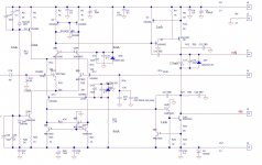
It's fairly well known on this forum that the Sloan CM'd complementary IPS doesn't work, which is why Bob Cordell added correcting devices, of which R13 and R15 are part. Shouldn't they be in yours?
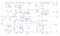
Thanks, I overlooked that. I put it in and here is the updated schematic.
So it works? I think so. It's the R14 and R16 that set the current limit on the VAS. Then the GNFB that control the ultimate voltage of the VAS.
Attachments
Last edited:
- Home
- Amplifiers
- Solid State
- Bob Cordell's Power amplifier book