There you go... I might use a trimmer there... The bias transistor is BC546 I shoud check things over again..
how to take a screen shot
An externally hosted image should be here but it was not working when we last tested it.
how to take a screen shot
Mihkus, This is potentially very good so it does deserve some proper thought. Unfortunately, having only got back in an hour ago, I'm not really able to give it that thought at the moment as I'm too tired to be sure of what I say.
There are problems with every configuration when it comes to layout. Off the top of my head i think I'm going to be concerned with the fact that the op amp, the most sensitive part of this circuit, seems to be surrounded by large currents and at the centre of this melee (mix).
Also though there is plenty of precedent for using bus-like power rails, they are usually about as bad as you can get, not least because the enclosed area is large. Ideally one wants everything twisted before it gets to the board and, once there, have the return paths closely coupled (ie nearby) to the power rails. One can do this quite neatly with a two-sided board.
The last thing you want (almost, perhaps) is the power for the op amp coming directly from your supply. Yes, you want separate branches but a single point star doesn't actually achieve that - or at least it can manage to make mistakes in doing so. Unfortunately, neither are Bob Cordell's solutions to grounding and power the final word on it. One also needs to do the same sort of stars with the + and - supplies and an immense amount of thought needs to go into how you are going to position your grounds, especially when it's not a balanced system. Do you want to have the ground set and attached to the case at the entrance of the signal, and perhaps have an on-board ground protected by a 10 ohm resistor. (This is awfully annoying when you want to build the circuit first and leave the case until last, and be able to play music on just a board.)
I have got to have a think about how one bypasses the op amp (and I haven't looked at its circuit for clues yet) but there are a couple of different ways - through to ground plane for bypass or to local ground? There is a huge temptation to go directly to a ground plane which I expect I will one day not overcome.)
Anyway, each of these thinking about properly, probably doing some sketches of where the current is flowing and probably me having to look at how I'd lay out this amp. I'm not saying that what I see wouldn't be a f*** sight better than anything you'd get out f China, or even here, but half of the sound of an amp is in the way it is put together. I will come back when I have had some thoughts.
What would I need to change to make it as good as it possibly can be?
I can add 10 times the amout of components on board, but...
My mind seems to be clear of thoughts
I want to build this amp so badly! But I cant before my grounding is 100% CORRECT.
I already got all the components
Feels like chritsmas!
I can add 10 times the amout of components on board, but...
My mind seems to be clear of thoughts
I want to build this amp so badly! But I cant before my grounding is 100% CORRECT.
I already got all the components
Feels like chritsmas!
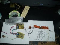
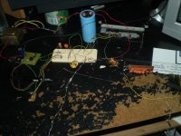
I bread boarded my version on a Protoboard to see if it would work first.
Then I drew it up the schematic in Circuitmaker2000 as it was before I tore it apart so that I could rebuild it later and work with it some more.
It is such a simple design that you should be able to breadboard the whole thing if you don't have a Protoboard and just have pigtails running to the output devices that are bolted to a heat sink of some sort.
A very big heat sink wouldn't be needed for testing purposes since it will be only about 10 to 30 watts of power and a piece of aluminum plate will suffice.
If it starts to get to warm then throw a small fan on it, You would be quite amazed at what a difference it would make.
I did that while I was designing my Variable HV power supply while I was in the designing stage and was running the FET's as high as 100c and just a little fan kept them cool below about 65c to 50c or less and they were just mounted on a piece plate aluminium at the time.
Here is a picture of how rough the layout was and I used the same heat sink and protoboard for the amp as well.
http://www.diyaudio.com/forums/plan...tor-insulation-mylar-coating.html#post2773108
Does anyone have schematics of a varible HV power supply
jer")
Then I drew it up the schematic in Circuitmaker2000 as it was before I tore it apart so that I could rebuild it later and work with it some more.
It is such a simple design that you should be able to breadboard the whole thing if you don't have a Protoboard and just have pigtails running to the output devices that are bolted to a heat sink of some sort.
A very big heat sink wouldn't be needed for testing purposes since it will be only about 10 to 30 watts of power and a piece of aluminum plate will suffice.
If it starts to get to warm then throw a small fan on it, You would be quite amazed at what a difference it would make.
I did that while I was designing my Variable HV power supply while I was in the designing stage and was running the FET's as high as 100c and just a little fan kept them cool below about 65c to 50c or less and they were just mounted on a piece plate aluminium at the time.
Here is a picture of how rough the layout was and I used the same heat sink and protoboard for the amp as well.
http://www.diyaudio.com/forums/plan...tor-insulation-mylar-coating.html#post2773108
Does anyone have schematics of a varible HV power supply
jer
Attachments
A couple of links to begin with:
I had no idea that you could get this online for free, but it's a fantastic book. The Art of Electronics. You need to go to page 407 or thereabouts for signal grounding. (The scribd and the real page numbers don't line up - it's actually page 457 in the book)
Also, for speccing out your board, this is invaluable. You can then put proper values of resistance and inductance into your LTspice schematic.
Saturn PCB Design - PCB Via Current | PCB Trace Width | Differential Pair Calculator | PCB Impedance
There seem to be an awful lot of mistakes on this board. I don't know what those resistors between the power transistor bases and V+- are. There was some mistake on the drivers going to rails as well. I don't know that you need the drivers on the heatsink. The more usual layout is that you have the emitter resistors where those drivers are, any if anything more than a localised h/sink is required, which can be flat on the board, then you put a bar across the two of them. I'm not sure those drivers can really take all that is going to be thrown at them, but it was hard to find anything but a scrappy datasheet, and I must check again how much power they are dissipating.
Now, you do know that those drivers are discontinued, don't you? Not that they are a critical part, though if they do get too fast, you may want to leave room for a stopper resistor of 2 to 5 ohms on the bases of the power trannys.
I don't really see anything I have suggested on the input being allowed for. You may as well include them on the board - they are all there to improve things - even if you don't end up puting them in place straightaway. Quickly on the bypass caps for the op amp. It's quite a meaty thing and I would have thought that something like a 2.2uF tantalum would be a good start, each going to ground. You might want to leave room for some cOg caps - maybe 0.47u - in parallel with them and also leave a space for a cap to go from rail to rail, directly across the op amp.
I don't see much in the way of the feedback loop, and certainly don't see it executed properly - nor do I see a zobel, let alone a R//L (which I know wasn't on the schematic).
The arrangement of the f/b should be that the two emmiter resistors meet in the middle (as on the sch), but you don't take the feedback from that point. A bit of track should go off to the tag or hole for the speakers, passing the zobel on the way, and then you take the feedback from after this. That zobel must go back to the main ground, not something more local and definitely not just across the loudspeaker terminals!
On the Vbe multiplier, I suspect that the best thing to do, is, where you have the T on the track, coming from the base. Put a 1k trimmer with the wiper going to the base. Then you'll need 470 on one side (across be) and perhaps 2k2 on the other. That gives you anything from 6:1 to 1.5 to one. There may be better values but that comes off the top of my head.
You don't actually have much of an issue with the grounds at the moment since the op amp doesn't have one, most of the amp doesn't reference one and it's only the input and the capacitors that actually go there. But nonetheless, you are enclosing a very wide area between the two rails and the ground paths. Ideally this area should be near zero and V+ and its return path should follow each other.
What I don't like about this is that we have different lengths of track going to each of the transistors, and I don't see that there is a consistency in track widths when Current in equals Current out. Very little is going to go across the capacitors, though it is worthwhile (though hardly critical) making their path to ground short and fat, because otherwise it just adds to the ESR otherwise. Saturn will tell you by exactly how much. It depends on what 100uF caps you have got.
This may not be ideal, and I haven't sketched this out, but one possible way is to have the rails go between where the two Res are now and then branch out to the collectors . The Rs get moved to meet in the middle, which is going to be near your o/p+ The two caps come together somewhere in the middle also, and that creates your power ground. A branch off that, or a tag/turret is o/p- coming back from the speaker.
From there, I would bring back V+ and V-, and I really would put in some regulation. LM337 and LM338 will make a hell of a difference to this, especially as you start drawing huge amounts of current. If you can't lose 3 volts from it you could use an LT308x, but they are quite pricey and doing the neg rail will not be easy. This new supply powers the Vbe multiplier and the op amp. Personally I would put in room for either another op amp or a card that can take power and perhaps has just the coupling cap on it. You do really want a consistent input resistance and I don't see one on your board. If you have one at 18k or so, then 1uF is not going to be enough. A 10uF Oscon, ZA or, if you like the Naim sound then a tantalum will be just fine. Otherwise nothing less that 2uF in foil. Alternatively you can put the input Z up to 47k, which is sort of the old standard.
But at the very least on the power going to the op amps etc, have a resistor and C, or a RC and zener, as is shown on the schematic. Incidentally 120R may be a bit high if a lot of current is demanded from the op amp, but it does make a very good current limiter.
One other thing, though they are not my favourite things. You might want 100uF from the 1k1 resistor to ground to reduce the gain to 1 at DC. There should be no need for it, but under fault conditions it means you don't get 20V DC at the output.
Now, I'll leave it to your artistry.
Last edited:
Move the +ve and -ve supplies to right next to each other.
Move the Power Ground to right next to the +ve & -ve supplies.
All high current traces from these 3 inputs must be "close coupled" to minimise radiated fields. Try to close couple the low current traces to the front end of the amplifier. The best location for this triplet of inputs is usually right next to the main output devices. Do NOT spread these 3 inputs around the PCB and do NOT enclose large loop areas inside the high current traces.
Quick note to say that the 1k1 f/b resistor will have to be quite a meaty thing, or put two 2k2 in parallel. If your supplies go up from the suggested 26V then it might end up dissipating about 1W.
I also missed saying what to do with the remainder of connections to Gnd. Basically bring a short fat track off from this power ground and create a brand new star ground for all the connections to ground, each going separately to this new point, and making sure that the ground reference from your regulator/zeners, goes to this point. From the V+ output of the regs have separate paths to the Vbe multiplier and the op amp, coming from the same point. Two other things on the Regs, you'll need about 1/2uF (anywhere from 0.1 to 1uF) on the input to them. Also they are better with a zener underneath them, the larger the better.
If you don't like big fat output resisistors Dale do some planar types which are fantastic. In 3W and, I think 5W. They come in strange values, like 0.2 or 0.5, but they can be had from Farnell at any rate. Not cheap though.
And while I remember, leave room for a tiny cap in parallel with the 22k f/b resistor. It shouldn't be needed but one may as well have a place for it. And if you are going to use SMD resistors, think about getting the meatier ones. Although they should have a TC of 25ppm or better, they have much less thermal mass so get hotter quicker.
My comments in post69, require the binning of the proposal and 90% of the other PCB layouts I see posted on this Forum.
It seems that few Builders understand the problem of radiated interference from the high current supply rails and wires.
Start again from a blank sheet of paper and pencil in device locations and trace routes. A pencil and eraser, at least for me, is far quicker than scrapping, time after time, CAD trial layouts.
Is the feedback resistor that sees the high voltage from the output rail 22k or 1k ?Quick note to say that the 1k1 f/b resistor will have to be quite a meaty thing, or put two 2k2 in parallel. If your supplies go up from the suggested 26V then it might end up dissipating about 1W...........
.............. leave room for a tiny cap in parallel with the 22k f/b resistor. ..... ........
Run both the lower leg and the upper leg resistors of the feedback loop at <<50% rating. I aim for <10%
26Vac and 22k results in ~30mW therefore use >300mW resistor. If the resistors have dubious HV rating then use two in SERIES. i.e. a pair of series connected 1/8W SMT will do better than a 1/2W SMT.
Andrew, I'm not thinking straight. I was thinking it was coming back to an LTP (which it is, in fact) but one that might have shown the full swing, which of course it won't - it'll get a 20th of it.
The advantage of parallel is that you effectively halve the TC. In series it stays the same. I feel fairly sure that the reason people don't go for the sound of sm resistors is that their temperature gyrates wildly and they don't have any other things like paint or epoxy or a core to give some thermal stability and keep them at a decently mean temperature. The only thing to conduct away the heat is the copper and that's >100 times worse at 3900ppm.
Did you mean we had to bin my proposal, or the board that Mihkus had put up? I was trying to let him down gently, given all the work he had done
Mihk's proposal has very widely separated +ve and -ve and Power Ground inputs with enormous loop areas.
That is what should be binned.
There are a number of other very experienced PCB designers that make the same mistake repeatedly even though I and others have suggested changing from that practice, but still it goes on.
No wonder beginners start thinking that those PCB layouts are good !
What do you mean "TC" is halved for paralleled resistors, but not for series resistors?
I knew this board was rubbish!
Making new one already Not mad but too damn tired
Just give me a picture of a proper PCB design that i should try to mimic or replicate...
Ive been checking those PeeCeeBee and VSSA designs...
I dont see any reason to use those lossy, big and badass resistors, If they give any kind of stability I dont need... Im pretty much like Frankenstein of electronics engineering....
Will my output transistor blow apart if i remove them? Probably not?
That could save shitloads of space... Cant get good ones too, those with minimal waste of space....
There are 5W ones with 7,5mm lead spacing and height of only 22mm These would be perfect! but cant get them
I need to think before I start making something... I sometimes think half a year before i build something..
Sometimes I just go for it, But WOW! my 2 way HiFi floorstanders project has been half done for half a year!
I even have the drivers, crossover parts, wires, screws, tools materials and even paint and varnish!
Going to have a walk, cant think anymore.
Making new one already
Not mad but too damn tired Just give me a picture of a proper PCB design that i should try to mimic or replicate...
Ive been checking those PeeCeeBee and VSSA designs...
I dont see any reason to use those lossy, big and badass resistors, If they give any kind of stability I dont need... Im pretty much like Frankenstein of electronics engineering....
Will my output transistor blow apart if i remove them? Probably not?
That could save shitloads of space... Cant get good ones too, those with minimal waste of space....
There are 5W ones with 7,5mm lead spacing and height of only 22mm These would be perfect! but cant get them
I need to think before I start making something... I sometimes think half a year before i build something..
Sometimes I just go for it, But WOW! my 2 way HiFi floorstanders project has been half done for half a year!
I even have the drivers, crossover parts, wires, screws, tools materials and even paint and varnish!
Going to have a walk, cant think anymore.
Last edited:
Mihk's proposal has very widely separated +ve and -ve and Power Ground inputs with enormous loop areas.
That is what should be binned.
What do you mean "TC" is halved for paralleled resistors, but not for series resistors?
That's what I said in No. 68 "But nonetheless, you are enclosing a very wide area between the two rails and the ground paths. Ideally this area should be near zero and V+ and its return path should follow each other."
The TC is halved in parallel because you get half the disippation, Ie Delta T, in each R. In series you get the same, but being in series they then add up to give you what you had before.
Mihkus,
Simply start with a two-sided PCB and keep the top side as mostly a large ground plane. That will almost-automatically minimize the loop area for the input signal/ground pair (minimizing its potential to be a receiving antenna) and the V+/Gnd and V-/Gnd pairs (minimizing their potential to be transmitting antennas), since they will always be right next to the ground that's on the other side of the board.
It doesn't seem like V+ and V- would ever act as a pair (for push-pull at least) so you should be able to route them apart from each other, however you want, if you have a ground plane. But I guess I could be wrong about that. It depends on the amplifier topology/class, too, I guess.
Using a ground plane would certainly make routing a lot easier and more elegant. And if you are making the PCB by hand, it's not much more difficult than a one-sided board. The only thing to actually worry about would be when planning to solder on the top side: You have to make sure that the component lead or pin will be accessible, there. If not (such as under a large electrolytic or a terminal block or a chip socket), then you can simply solder it on the bottom and also run a short trace (on the bottom side) out from under the component and make a via, into which you insert a short bare wire and solder on both the top and bottom sides. But if you were going to have the board professionally fabricated, then you'd have plated-through holes and wouldn't have to worry about anything like that.
You could make two ground planes: one smaller one for the opamp input circuitry and one for everything else. They would have separate connections back to the star ground point. That would probably be easiest to get right. The input ground wouldn't even necessarily have to be a plane. Or it could be a small one. It's good to run one under and all around any components that are in series with the input signal. Maybe you could use a third ground plane for the lowest-level transistor input signals. I don't know how that's usually done. But the idea is to keep the very large or very fast-changing other ground-return currents in their own separate conductor(s), on the way back to the star ground, so that the voltages they induce across the conductors themselves won't bounce your input signal ground reference points.
Cheers,
Tom
Last edited:
Is TC the temperature coefficient or the ceramic substrate temperature?...........The TC is halved in parallel because you get half the disippation, Ie Delta T, in each R. In series you get the same, but being in series they then add up to give you what you had before.
Temperature Coefficient. Change in resistance for every Deg C change in temperature.
It has frightening consequences, especially if it's short term. You can lose three and a half bits in a 16 bit system quite easily by mismatching it around just one op amp.
The way to look at it, assuming that R and Temp are linear, which they by and large will be, is to look at I^2 R. Put them in parallel and while you double the individual resistance the power falls off as the square, so giving you half. When those are put in parallel you still have the same percentage change as you would with half the current. In series you have the original change as you still have the same current and the same total resistance. (It's good also for inductance in speakers. And since properly big power resistors can be horribly non-linear, good to get over that too.)
Funnily enough I worked it out so long ago that I wasn't even sure, when you questioned it, whether I'd still have the answer. But it still stands up.
Last edited:
- Status
- This old topic is closed. If you want to reopen this topic, contact a moderator using the "Report Post" button.
- Home
- Amplifiers
- Chip Amps
- opamp plus driver stage and output stage with its own supply, what could happen?