at a guess, very very small is probably right.
If one looks at 1nH per mm for a "narrow" wire connection, then a die to backplate connection must be in the sub mm length, resulting in sub 1nH inductance.
If one then uses a "wide" wire, then the connection inductance is reduced.
The width of the die to backplate connection must be in the "wide" category.
Taking these conjectures together, I guess (again) that we are talking <<1nH
Is that <0.1nH (100pH) or < 0.01nH (10pH)
I have a friend who measured 1.3nF between source and heatsink, so it is apparently highly variable. I am wanting to try some methods that reduce the gap between the transistor and heatsink as much as possible and so capacitance and thermal conductance should be very high. For source-tab FETs, this is not really a problem because the output needs to be decoupled at RF anyways - this is in fact probably the best way to do it.
The very best way might be to use a lossy insulator like graphite, in addition to another insulator, so that the graphite provides direct damping right where it's needed. However I don't think this would be an improvement if the loop path were larger than the size of the necessary resistor. Still, maybe the graphite could act as a lossy ground plane around the device inductances?
The very best way might be to use a lossy insulator like graphite, in addition to another insulator, so that the graphite provides direct damping right where it's needed. However I don't think this would be an improvement if the loop path were larger than the size of the necessary resistor. Still, maybe the graphite could act as a lossy ground plane around the device inductances?
Last edited:
Minor loop gain inconsistency.
Bob, something for you and other interested parties to ruminate and cogitate over:
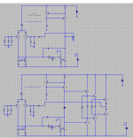
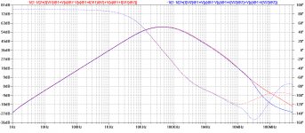
I have run a simulation of the minor loop gain of the generic single-pole Miller compensated amplifier with an ideal output stage in the form of a VCVS, and with an output stage using transistors configured in the Locanthi topology.
The problem here is I obtain a phase margin of 76 degrees with the ideal output stage and only 27 degrees with the non-ideal ouput stage. Any ideas on why this is the case?
It seems to me the phase margin obtained with the ideal VCVS output stage is the more realistic figure.
I have attached the .asc and the relevant SPICE models for your convenience.
Bob, something for you and other interested parties to ruminate and cogitate over:
I have run a simulation of the minor loop gain of the generic single-pole Miller compensated amplifier with an ideal output stage in the form of a VCVS, and with an output stage using transistors configured in the Locanthi topology.
The problem here is I obtain a phase margin of 76 degrees with the ideal output stage and only 27 degrees with the non-ideal ouput stage. Any ideas on why this is the case?
It seems to me the phase margin obtained with the ideal VCVS output stage is the more realistic figure.
I have attached the .asc and the relevant SPICE models for your convenience.
Attachments
I have a friend who measured 1.3nF between source and heatsink, so it is apparently highly variable. I am wanting to try some methods that reduce the gap between the transistor and heatsink as much as possible and so capacitance and thermal conductance should be very high. For source-tab FETs, this is not really a problem because the output needs to be decoupled at RF anyways - this is in fact probably the best way to do it.
The very best way might be to use a lossy insulator like graphite, in addition to another insulator, so that the graphite provides direct damping right where it's needed. However I don't think this would be an improvement if the loop path were larger than the size of the necessary resistor. Still, maybe the graphite could act as a lossy ground plane around the device inductances?
One amplifier company I once consulted for used thick anodization of the aluminum on the heat sink as the insulating barrier, and achieved very low thermal resistance. I'm guessing this might have been an instance where the tab-to-heat sink capacitance was high. Of course aluminum oxide anodization pinholes are a danger in such a design. I don't recall if the design using just anodization ever went into production.
Cheers,
Bob
Mike, it seems in YOUR world, 'ideal output stages' are always more 'realistic' than stuff which mere mortals and other gurus think closer to 'real life'.I have run a simulation of the minor loop gain of the generic single-pole Miller compensated amplifier with an ideal output stage in the form of a VCVS, and with an output stage using transistors configured in the Locanthi topology.
The problem here is I obtain a phase margin of 76 degrees with the ideal output stage and only 27 degrees with the non-ideal ouput stage. Any ideas on why this is the case?
It seems to me the phase margin obtained with the ideal VCVS output stage is the more realistic figure.

You may like to do some 'real life' stuff to check your copious, erudite (??) & pedantic pontificating
I have a friend who measured 1.3nF between source and heatsink,
Maybe isolate the heatsink and bootstrap it to the output voltage?
jan
Bob, something for you and other interested parties to ruminate and cogitate over:
I have run a simulation of the minor loop gain of the generic single-pole Miller compensated amplifier with an ideal output stage in the form of a VCVS, and with an output stage using transistors configured in the Locanthi topology.
The problem here is I obtain a phase margin of 76 degrees with the ideal output stage and only 27 degrees with the non-ideal ouput stage. Any ideas on why this is the case?
It seems to me the phase margin obtained with the ideal VCVS output stage is the more realistic figure.
I have attached the .asc and the relevant SPICE models for your convenience.
Bob, the reason for my mystification is that firstly the output stage is outside the minor loop; secondly, shunt capacitance introduced by the input impedance of the output stage would be expected to increase minor loop stability margins and not reduce them.
Is it possible that the input impedance of the output stage "looks" inductive to the output of the TIS?
This, perhaps, may explain the deterioration in phase margin of the minor loop; however, it isn't intuitively manifest to me that this is the case.
Note that including 1K resistors in series with each input BJT of the output stage seems to resolve the issue, with minor loop gain being nearly identical in this instance with that obtained with the ideal VCVS, but for a small inexplicable resonant peak preceeding unity loop gain frequency.
Last edited:
Bob, something for you and other interested parties to ruminate and cogitate over:
I have run a simulation of the minor loop gain of the generic single-pole Miller compensated amplifier with an ideal output stage in the form of a VCVS, and with an output stage using transistors configured in the Locanthi topology.
The problem here is I obtain a phase margin of 76 degrees with the ideal output stage and only 27 degrees with the non-ideal ouput stage. Any ideas on why this is the case?
It seems to me the phase margin obtained with the ideal VCVS output stage is the more realistic figure.
I have attached the .asc and the relevant SPICE models for your convenience.
No relevance to the problem you re pointing (but who knows?)
but i suggest that you make tries with a voltage referenced CCS
as VAS/TIS load rather than an active source.
Goolge search: T0-247 lead inductance, 1st hit onsemi power mosfet datasheet
INTERNAL PACKAGE INDUCTANCE
Internal Drain Inductance
(Measured from the drain lead 0.25″ from package to center of die)
LD − 5.0 − nH
Internal Source Inductance
(Measured from the source lead 0.25″ from package to source bond pad)
LS − 13 − nH
...
You may like to do some 'real life' stuff to check your copious, erudite (??) & pedantic...
Seems to me that in this case Mike has perfectly politely asked a question to help understand better. Where is this pontification?
Your complaints have become indiscriminate to the point that they commit what they purport to condemn, unproductive repetition.
Some of Mike's controversies have been quite productive.
I prefer useful posts, so let's look at his query first.
Best wishes
David
I'm suitably reprimanded Mr. Zan .. though I'm less convinced about Mike's controversies.Seems to me that in this case Mike has perfectly politely asked a question to help understand better. Where is this pontification?
Your complaints have become indiscriminate to the point that they commit what they purport to condemn, unproductive repetition.
Some of Mike's controversies have been quite productive.
I prefer useful posts, so let's look at his query first.
But if I may enter a 'real life' point which most of us may find more important than sims or theory, the circuit as it stands, without Zobel or output inductor network is likely unstable while open circuit.
Only in my very limited experience of course.
I thank MikeK for his suggested 'cures' which of course need to be tried in 'real life'.
He might also like to look at http://www.diyaudio.com/forums/solid-state/234408-stability-analysis-ef-output-stages-2.html Again this is 'real life' stuff so may not be of interest .. and the conditions are not quite the same.
I (quite sincerely) hope this is useful.
Maybe isolate the heatsink and bootstrap it to the output voltage?
jan
Isolating the heatsink is an interesting idea but I think ultimately unnecessary; I'd like to avoid the hassle and safety concerns. Almost every amp needs an RC at the output for stability. The impedance null caused by the source-ground capacitance and loop inductance has always been disastrous in my prototypes. If the heatsink-PCB ground length is at least 5 times more than the length from heatsink to the RF ground of the output stage, then a resistor directly between the heatsink and this ground should be superb for stability.
So my idea is not to reduce or bootstrap the capacitance, but increase it along with thermal conductivity, and use it as the output RC resulting in a better amplifier in multiple areas.
Goolge search: T0-247 lead inductance, 1st hit onsemi power mosfet datasheet
The only caveat here is that the quoted drain inductance is from die to TO247 drain lead. I think the inductance of interest was the inductance directly downward from the die drain of the BJT to the heat plate on the backside of the device.
Cheers,
Bob
Isolating the heatsink is an interesting idea but I think ultimately unnecessary; I'd like to avoid the hassle and safety concerns. Almost every amp needs an RC at the output for stability. The impedance null caused by the source-ground capacitance and loop inductance has always been disastrous in my prototypes. If the heatsink-PCB ground length is at least 5 times more than the length from heatsink to the RF ground of the output stage, then a resistor directly between the heatsink and this ground should be superb for stability.
So my idea is not to reduce or bootstrap the capacitance, but increase it along with thermal conductivity, and use it as the output RC resulting in a better amplifier in multiple areas.
Yes that sound quite interesting too, although you still need to isolate the heatsink I guess? (But I may misunderstand you).
Well worth the try.
jan
One amplifier company I once consulted for used thick anodization of the aluminum on the heat sink as the insulating barrier, and achieved very low thermal resistance.... Of course aluminum oxide anodization pinholes are a danger in such a design. I don't recall if the design using just anodization ever went into production.
I have also considered to mount the transistors directly on anodised aluminium.
It looks very attractive in theory, excellent thermal conductivity for an insulator.
I am a bit nervous since I have no experience with actual practice.
Does any company do this? Or does anyone have information on this?
Best wishes
David
I have used anodized washers under the power transistor and mounted the heat-sink to the chassis via plastic/fiber shoulder washers. This puts the capacitance to ground in series and gave a low C result. Works fine. Allows for some extra margin for HF noise and distortion reduction. [it also keeps the chassis inside a little cooler... not heating up the whole chassis.]
Thx-RNMarsh
Thx-RNMarsh
Bob, the reason for my mystification is that firstly the output stage is outside the minor loop; secondly, shunt capacitance introduced by the input impedance of the output stage would be expected to increase minor loop stability margins and not reduce them.
Is it possible that the input impedance of the output stage "looks" inductive to the output of the TIS?
This, perhaps, may explain the deterioration in phase margin of the minor loop; however, it isn't intuitively manifest to me that this is the case.
Note that including 1K resistors in series with each input BJT of the output stage seems to resolve the issue, with minor loop gain being nearly identical in this instance with that obtained with the ideal VCVS, but for a small inexplicable resonant peak preceeding unity loop gain frequency.
Actually, shunt capacitance at the TIS output introduces a pole which reduces minor loop gain at HF and reduces minor loop phase margin as well.
If such shunt capacitance is used, then a small resistor should be connected in series with the shunt capacitor to introduce a zero near the unity minor loop gain frequency to enhance stability margins.
P.S. The "small inexplicable resonant peak preceeding unity [minor] loop gain frequency" appears to be due to Andy_C's output transistor models: MJL3281A_X & MJL1302A_X.
Otherwise, the minor loop transmission characteristic obtained with the ideal VCVS output stage is in fact the correct one as I suspected here:
http://www.diyaudio.com/forums/soli...lls-power-amplifier-book-433.html#post3640536
Last edited:
- Home
- Amplifiers
- Solid State
- Bob Cordell's Power amplifier book