Go head Bli John with your own design I am sure Shaan will glad to see it.Ok mas Thanks,
I want to make PCB that input pairs can use BC's pair or SA/SC pair so it can swap easily with different transistor. I'm an "orang lambat" so mine maybe not finish soon
Waiting for Shaan if he let my "hand made PCB" can be post here
Regards
Just remember to thermally coupled input pair. Make as short as possible track this is fast amp.
I've replaced trimmer with fixed resistor as close as I could.
Supply +-40vdc (32vac)
Dco 9-10mv
Vas bias ~10mA
Input bias ~2.3mA
And load with 4ohm (parallel 2 bookshelf), I can't believe my ears.. the sound was incredible. Crispy trebles, punchy bass, open mid... and relaxing sound.
Best sounding amp I've ever assembled so far.
Happy listening...

Thanks Naf, congratulation.
I must build this one
Please, can you tell me all transistors you use? Are they all matched?
cause I don't have pairs C grade BC's(only BC550C)
to Shaan it is OK if I post my PeeCeeBee design here?
(I want to made my own PCB layout)
Regards
Sure it's okay. It's a peeceebee so nothing to worry about!
And load with 4ohm (parallel 2 bookshelf), I can't believe my ears.. the sound was incredible. Crispy trebles, punchy bass, open mid... and relaxing sound.
Best sounding amp I've ever assembled so far.
And yet so simple, it really is a little wonder.

Thanks Naf, congratulation.
I must build this one
Please, can you tell me all transistors you use? Are they all matched?
cause I don't have pairs C grade BC's(only BC550C)
I suggest the input NPN/PNP transistor pair are BC550C/BC560C (or equivalents) to have high and equal hFE (beta - current gain) as much as possible. Normally both should have the same hFE=600 or more. Also the input pair must be glued together with their flat sides so they are in thermal contact and their hFE will change proportionally. This is important since symmetrical DC offset tracking for both positive and negative side of the VSSA is assured in that way, resulting in zero DC offset at the output.

Hi Shaan,
What are the FETs that can be used in your PeeCeeBee layout published in the first post ?
I will document it for future build.
Thank you very much.
2SK1058 and 2SJ162. You can use other power LATFETs in TO247/TO264 packages too if you want, with maybe some mods in the bias setting zone for setting the FET Iq.
It really is a little wonder.
Looking at the schema and layout many will just underestimate it, to their own miss.
And yet so simple, it really is a little wonder.
I suggest the input NPN/PNP transistor pair are BC550C/BC560C (or equivalents) to have high and equal hFE (beta - current gain) as much as possible. Normally both should have the same hFE=600 or more. Also the input pair must be glued together with their flat sides so they are in thermal contact and their hFE will change proportionally. This is important since symmetrical DC offset tracking for both positive and negative side of the VSSA is assured in that way, resulting in zero DC offset at the output.
Hi Lazy Cat thanks for the guidance, I try my best available part here
I hope can made it easy
Nice suggestion Shaan, for best result why not.Also, buiders are suggested to measure and match the feedback resistors in both polarity as close as possible(2K2/100R or 1K/47R), to balance the fb current resulting in highest attenuation of the even harmonics. However, this is not essential.
I'm also find how to match the resistor with cheap digital multimeter, we can apply enough voltage to resistor under test (if needed with series resistor to limit the current) & measure voltage on it by 200mV range
Btw what resistor you preferred cheap carbon matched or metal film matched on this fb position.
I have a few dale resistor somewhere
And one more thing, please link how to accurate matching input bjt, VAS, & output LAT FET
Last edited:
Btw what resistor you preferred cheap carbon matched or metal film matched on this fb position.
I have a few dale resistor somewhere
I have never used carbon resistors with VSSA, only metal film, 1% tolerance. Good enough.
And one more thing, please link how to accurate matching input bjt, VAS, & output LAT FET
I can't tell you that(I don't know any good online links on that). You need to ask LC, better to post your questions about matching and others in the VSSA thread.
Last edited:
Well, it looks like I'll have some more things to do.
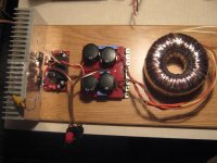
I removed cap multiplier. Now I have simple power supply with two Graetz bridges and 4x 6.800uF smoothing caps per channel. I can't hear any difference. Without signal, there's only silence: turn on, turn off, no buzz, no hiss, no brum, nothing. DC offset was zero without adding resistors. Perfect.
But...
Now VAS transistors begun to overheat. Again I had only few minutes to enjoy music.
So I removed trafo, put new one 2x 20VAC and got 25VDC per rail. Finally, everything was good, transistors almost cold, no problems except DC offset of 37mV. I'll solve it tomorrow.
Now I'm listening to music. This is very good amp, definitely it's value is greater then invested money. Like LC said "it really is a little wonder".
Attachments
@Shaan & others: Very impressive thread!
Q: Looks like you are encouraging people to modify your layout (please correct me if I am mistaken) in this thread, but not the schematic? I ask b/c I would probably change the shape of the board a bit for my own personal use, but don't like to step on toes in what is already an awesome thread...
Q: Looks like you are encouraging people to modify your layout (please correct me if I am mistaken) in this thread, but not the schematic? I ask b/c I would probably change the shape of the board a bit for my own personal use, but don't like to step on toes in what is already an awesome thread...
@Shaan & others: Very impressive thread!
Q: Looks like you are encouraging people to modify your layout (please correct me if I am mistaken) in this thread, but not the schematic? I ask b/c I would probably change the shape of the board a bit for my own personal use, but don't like to step on toes in what is already an awesome thread...
Hi PMI.

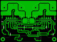
I published the layout because I got requests for one in the VSSA thread and PM.
It is very compact and has non-polar electro at the input, I didn't add Zobel and Cdom(intentionally) for keeping it as small as possible(for me). My story ends here.
But each diy-er has his/her own circumstances/requirements, under which they design their own peeceebees and post them here. If my layout satisfies their needs then they might use it as it is, or, make their own based on the same schematic(yes, the schema is fixed
).It's fun and all are welcome.
I just want to encourage fellow guys here to try this tiny little amp and get shocked by the sound it produces for the bucks invested. I'm confident that everyone who tries peeceebee, will be satisfied(nothing is being sold here b.t.w.
)shaan
Now I'm listening to music. This is very good amp, definitely it's value is greater then invested money. Like LC said "it really is a little wonder".
Enjoy!
Little wonder indeed. My friends here went "WHA... this is impossible" when they discovered that the veroboard that was rattling the house isn't a class-D and is only 2"X3" and has only four BJTs on board.
Well, it looks like I'll have some more things to do.
I removed cap multiplier. Now I have simple power supply with two Graetz bridges and 4x 6.800uF smoothing caps per channel. I can't hear any difference. Without signal, there's only silence: turn on, turn off, no buzz, no hiss, no brum, nothing. DC offset was zero without adding resistors. Perfect.
But...
Now VAS transistors begun to overheat. Again I had only few minutes to enjoy music.
So I removed trafo, put new one 2x 20VAC and got 25VDC per rail. Finally, everything was good, transistors almost cold, no problems except DC offset of 37mV. I'll solve it tomorrow.
Now I'm listening to music. This is very good amp, definitely it's value is greater then invested money. Like LC said "it really is a little wonder".
If dc offset is only 37mV it probably won't hurt any loudspeaker.
One more very important info for all VSSA PeeCeeBee builders. Please install as best as possible 2,2 mF/6,3 V capacitor (Nichicon FG, Elna Silmic, etc) if possible paralleled with 10 uF/MKT (Vishay, Epcos, etc.).
Sound will change very dramatically in the first 10-20 listening hours because of this capacitors, so be generous and give enough time to VSSA to settle down.
Sound will change very dramatically in the first 10-20 listening hours because of this capacitors, so be generous and give enough time to VSSA to settle down.
Hi Tyimo.
It's just different perspectives. It's the same thing. Notice the order - for the positive polarity npn input bjt collector to pnp vas bjt base, for negative it's pnp input bjt collector to npn vas bjt base.
I re-arranged the original placement of the input stage so that all the transistors that processes the +ve part of the signal remains above the ones processing the -ve part. To me this makes it look better and easier to digest.
shaan
- Home
- Amplifiers
- Solid State
- PeeCeeBee