Don't plug speakers into that! And be careful without them plugged in. Something's obviously wrong with your circuit, and you might find your quiescent current could be too high - which could cook your output transistors. Do you have very low resistance in the power rail (I think my JLH 96 has 0.33ohm power resistors - they were in the original circuit). You could check the voltage across those and calculate the Iq to rule out it being too high.
Check the circuit. Are you happy the variable resistances are wired the right way? Are all your transistors wired up as you expect?
Check the circuit. Are you happy the variable resistances are wired the right way? Are all your transistors wired up as you expect?
Looks like the orientation of VR3 may be wrong?
An externally hosted image should be here but it was not working when we last tested it.
Looks like the orientation of VR3 may be wrong?
An externally hosted image should be here but it was not working when we last tested it.
Anyone?
It seems from the mask that the adjusters are linked to the series resistors?
An externally hosted image should be here but it was not working when we last tested it.
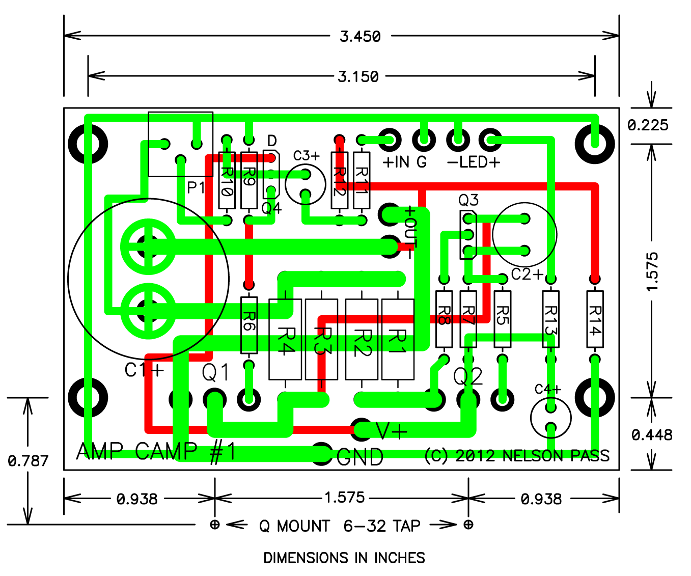
I do not get it, the actual board this guy soldered is not the same as in the picture. The output transistor pins are not in a line as in the soldered board. On the PCB layout picture output pins are in the triangle, and not in a line.
Lets hope here are no mistakes after all.
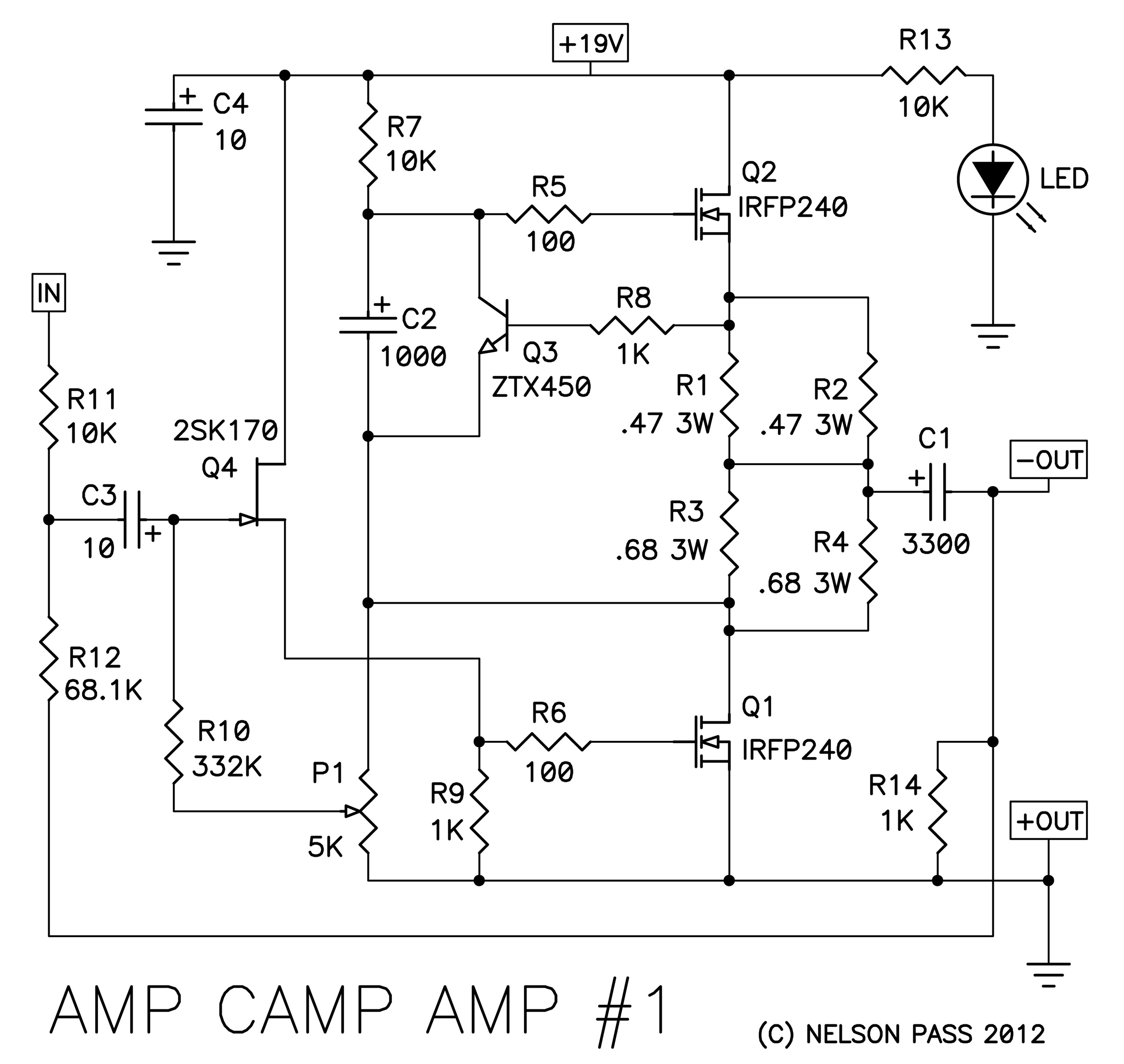
Same is with AmpCampAmp board. Does not match with the schematic given P1 goes to + of output Cap on the PCB, but not the schematic. Sorry for off topic. I hate mistakes Check what you have got.
Lets hope here are no mistakes after all.
Same is with AmpCampAmp board. Does not match with the schematic given
P1 goes to + of output Cap on the PCB, but not the schematic. Sorry for off topic. I hate mistakes Check what you have got.
Note that all three adjust pots have two leads/legs connected by a trace.
This converts all three pots to variable resistors. Post2647 is different !!!!!
When the pot is a variable resistor then the direction of rotation of the adjust screw changes with the orientation of the pot.
The designer can, if he/she wishes arrange for the resistance to increase with clockwise rotation of the adjuster.
Or, just as valid, that the parameter that is affect by the adjustment increases with clockwise rotation of the adjustment screw.
Equally the designer could swap the pots around for anticlockwise to achieve the same.
The Builder has a choice:
a.) do it the way the designer shows.
b.) do it the way the designer intended.
c.) do it the way it makes sense to you as the builder/operator.
Last edited:
Thanks Andrew. I was going to originally ask if the orientation of VR1 - 3 made any difference. However I assumed by post 2643 that it did. So it seems you cannot get it wrong? If that is so, then I have problems elsewhere.
Rob.
Rob,
I have the same kit from Siliconray that I bought sometime ago and am still working on it. I noticed that the 3 trim pots (VR1 VR2 and VR3) that you used are different from mine. Did you buy the whole kit or did you just get the board? In my kit, the pots can only go in one way and they fit the outline on the board exactly.
Regards,
Lo_Tse
Hi
What values of resistor have you got for the input bias adjuster (would this be VR1?). If I add up the currents there is roughly 350 uA in the input transistor plus a bias across the 2.7k feedback resistor which will be another 250uA or so, totalling 600uA in the first stage bias. Therefore you should have a resistor of about 1k which suggests we need a variable of about 2.2k and a series limiting value of maybe 220 ohms.
On the other hand if the feedback decoupling capacitor is eliminated (feedback grounding resistor connected directly to ground) then 10 times more current is needed.
Is it that the input resistor-variable resistor is mismatched to the circuit (i.e. values for no capacitor used with a decoupling capacitor?)
CHeers
John
The problem I see is this: using the Siliconray drawing of JLH's 2005 amplifier (and just how are the components labelled?- I normally start with R1, Tr1 on the left and work left-to-right, top-to-bottom) VR1 sets the current in the input transistor. Its emitter voltage should be around +.7V because the base is tied to ground through bias resistors R2,R3). If C3 is included, the current flowing in R8 (feedback resistor) is about 250uA or so. The current flowing in the first stage transistor (I'd call this Tr1, not Q4, and redraw the circuit so that Q5 and Q6 were a little more to the right!) is about 150uA, plus whatever base current is needed by Q3. Therefore the emitter resistor of Q6 should be about 0.65/.45mA or 1.4k. If C3 is omitted (shorted) then R6 conducts about 3mA, making the sum of R13 plus VR1 about 200 ohms. It is unclear what VR3 does but might be used to provide some sort of temperature compensation.
HOwever, on second thoughts, my proposal that if you use C3 wiht component values as given (VR1=200) then the output voltage will be about -7V not +7V. IS this the case?
If not then I suspect that a transistor may be wrong (7V is a zener voltage of a reversed base-emitter junction). Have you inadvertently used a BD139 where Q8 should have a BD140 or something?
In any case, you have a choice. Either remove C3 (and replace with a jumper wire) or replace R13 with a 220 ohm and VR1 with a 2.2k pot. Siliconray or whoever should have pointed this "howler" out. C3 might be optional but needs different resistors.
Cheers
John
The BOM specified these values -
VR1 200
VR 250
VR3 20k
Hi, Puffin
According to the BOM that came with my kit:
VR1 - 200
VR2 - 50
VR3 - 20K
Hope this helps!
Regards,
Lo_Tse
Hi, Puffin
According to the BOM that came with my kit:
VR1 - 200
VR2 - 50
VR3 - 20K
Hope this helps!
Regards,
Lo_Tse
Sorry VR2 is 50r (it was very early when I posted
)Rob.
The problem I see is this: using the Siliconray drawing of JLH's 2005 amplifier (and just how are the components labelled?- I normally start with R1, Tr1 on the left and work left-to-right, top-to-bottom) VR1 sets the current in the input transistor. Its emitter voltage should be around +.7V because the base is tied to ground through bias resistors R2,R3). If C3 is included, the current flowing in R8 (feedback resistor) is about 250uA or so. The current flowing in the first stage transistor (I'd call this Tr1, not Q4, and redraw the circuit so that Q5 and Q6 were a little more to the right!) is about 150uA, plus whatever base current is needed by Q3. Therefore the emitter resistor of Q6 should be about 0.65/.45mA or 1.4k. If C3 is omitted (shorted) then R6 conducts about 3mA, making the sum of R13 plus VR1 about 200 ohms. It is unclear what VR3 does but might be used to provide some sort of temperature compensation.
HOwever, on second thoughts, my proposal that if you use C3 wiht component values as given (VR1=200) then the output voltage will be about -7V not +7V. IS this the case?
If not then I suspect that a transistor may be wrong (7V is a zener voltage of a reversed base-emitter junction). Have you inadvertently used a BD139 where Q8 should have a BD140 or something?
In any case, you have a choice. Either remove C3 (and replace with a jumper wire) or replace R13 with a 220 ohm and VR1 with a 2.2k pot. Siliconray or whoever should have pointed this "howler" out. C3 might be optional but needs different resistors.
Cheers
John
Hi John, thanks very much for your reply. I will do some checking and report back. It might take a few days as I don't have a lot of time at the moment.
Rob.
UPDATE :
I removed C3 (after having checked the values of VR1, 2 & 3 as I had not in fact checked them before installing) they were fine. Fired it up and started to adjust the DC offset (no speakers within 100 miles)
Got it down to 0 and attached speakers. Offset seems to drift, but nothing more than 50mv.
Is it a matter of continually adjusting or where is it best advised to leave it?
A big thank you to John_ellis for his advice.
Rob.
I removed C3 (after having checked the values of VR1, 2 & 3 as I had not in fact checked them before installing
) they were fine. Fired it up and started to adjust the DC offset (no speakers within 100 miles)Got it down to 0 and attached speakers. Offset seems to drift, but nothing more than 50mv.
Is it a matter of continually adjusting or where is it best advised to leave it?
A big thank you to John_ellis for his advice.
Rob.
- Home
- Amplifiers
- Solid State
- JLH 10 Watt class A amplifier