Latest
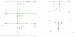
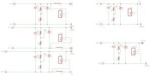
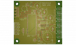
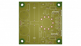
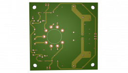
OK, here is where I am now. I have made some changes to the circuit. I am now using a 74hc4040 to divide bclk by 8 which should give 4fs to 8fs in most situations. This is optional however, as one could, I suppose, bridge across the 4040 without installing it. I have to admit I have a very basic understanding of the logic chips.
As another option, one could forgo the logic chips and instead use R17, C25, C26, and D1 on the bottom of the board and perform a grundig style DEM connection. I have read recently how some prefer that style.
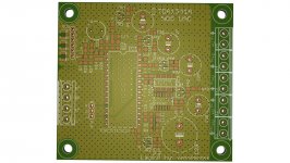
As far as the size of the board. As it is now it is 3.2 x 2.9 inches.
Terminating the u.fl with resistors is no problem, just need to determine the proper placement. Is there any situation where terminating it could cause a problem?
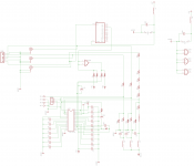
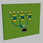
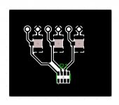
Sorry about the messy schematic, it has been through many revisions. Will clean it up when boards get made.
As always critique is welcomed.
Thanks,
Chris
OK, here is where I am now. I have made some changes to the circuit. I am now using a 74hc4040 to divide bclk by 8 which should give 4fs to 8fs in most situations. This is optional however, as one could, I suppose, bridge across the 4040 without installing it. I have to admit I have a very basic understanding of the logic chips.
As another option, one could forgo the logic chips and instead use R17, C25, C26, and D1 on the bottom of the board and perform a grundig style DEM connection. I have read recently how some prefer that style.
As far as the size of the board. As it is now it is 3.2 x 2.9 inches.
Terminating the u.fl with resistors is no problem, just need to determine the proper placement. Is there any situation where terminating it could cause a problem?
Sorry about the messy schematic, it has been through many revisions. Will clean it up when boards get made.
As always critique is welcomed.
Thanks,
Chris
Attachments

OK, here is where I am now. I have made some changes to the circuit. I am now using a 74hc4040 to divide bclk by 8 which should give 4fs to 8fs in most situations. This is optional however, as one could, I suppose, bridge across the 4040 without installing it. I have to admit I have a very basic understanding of the logic chips.
As another option, one could forgo the logic chips and instead use R17, C25, C26, and D1 on the bottom of the board and perform a grundig style DEM connection. I have read recently how some prefer that style.
As far as the size of the board. As it is now it is 3.2 x 2.9 inches.
Terminating the u.fl with resistors is no problem, just need to determine the proper placement. Is there any situation where terminating it could cause a problem?
Sorry about the messy schematic, it has been through many revisions. Will clean it up when boards get made.
As always critique is welcomed.
Thanks,
Chris
As far as terminating the ufl, from an rf perspective I just don't see how you wouldn't terminate them unless whats driving them isn't set at the right output impedance, this is all to minimize reflections.
But also are you 100% sure you want to make PCB's with the thru-hole logic chips? Really the potato chips are the way to go as some measurements in another thread recently showed. With digital smaller footprint is always better.
Also I believe now I see what 3setup was refering to with the cut ground plane, its the VR's. You want as much groud plain retuning currents as possible, this is where a 4 layer board comes in handy, but at at some point it just becomes easier to build PTP on a pored copper ground plain in 3 dimensions.
I guess if I had the patience to work with PCB software I would do 4 layers and use better regs than the TL431's but I uderstand the time involved, what you have is a big improvement over the red baron boards as is. But if you want to go that direction (4 layer pcb) I have some snippets saved that explain the current flows around the TDA and the better 4-layer practice I could email you, shoot me a PM if you want.
Latest
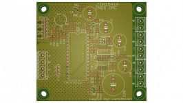
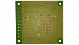
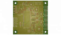
Here is a version with expanded unsplit bottom ground plane.
I'm not sure what you mean by thru-hole logic as I changed to smt already. If the the potato chips are better, I have no problem changing. Which chip would be better for the 74hc4040 divider, or is that good as it is?
Here is a version with expanded unsplit bottom ground plane.
I'm not sure what you mean by thru-hole logic as I changed to smt already. If the the potato chips are better, I have no problem changing. Which chip would be better for the 74hc4040 divider, or is that good as it is?
Attachments
Some reason I can't edit my last post, but I forgot to ask which VR would be recommended over the tl431? Is there is a consensus?
Also, aren't the potato po74g02 pin compatable with the smt 74hc02?
And for terminating the u.fl I would just use a 50 ohm from signal to ground right?
Thanks,
Chris
Also, aren't the potato po74g02 pin compatable with the smt 74hc02?
And for terminating the u.fl I would just use a 50 ohm from signal to ground right?
Thanks,
Chris
Last edited:
Is the TL431 really a good choice? If you went smt with potado logic and dropped the TL431's you could have a really small board that could butt right next to salas regs.
I know that TL431 with TDA1541 sounds much better than a board without TL431.
Tried both. No contest.
Is there better? Not sure. You tell me..
Latest
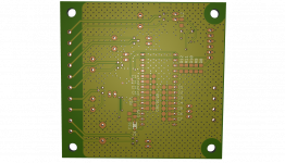
OK, here we are with the latest. I have added 2pin headers for each supply. This, I think, is the best compromise as it should allow the use of the Salas regulators voltage sense function and just use the normal headers for the supply. From what I can tell, one of the primary benefits of the Salas regs is the remote sense function which allows for the regulator to be some distance from the load. Or, one could use ccs supplied tl431, or a combination. I don't want to go only Salas regulators as I don't have any currently
As far as terminating the i2s signals, from what I have found that is done on the source side with 22 ohm resistors usually, so barring other info I will leave it off.
So, I think I will move forward with this one, unless some other errors are found. I guess post if interested in the board though I'm not sure what kind of initial run to do. I think it will depend on how many people are interested. I would like if a few people with test equipment and the desire to test would be involved.
Thanks,
Chris
Attachments
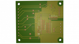
Well they started there from an earlier version of the board which had more ps components at the end of the chip, but I'm not sure it would matter greatly. I could run them out the end of the chip now, but that would disrupt the ground plane from pin 14 to the supply. So either way I think it is a trade off, and I think disrupting the ground plane may be worse. Not sure why the trace thickness need increasing. They are significantly larger than the signal requires. How many mills do you think they should be?
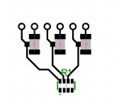
I must admit to still being a bit confused as to why the pinheader is after the ufls, why not before and have the u.fl facing the other direction? particularly if anyone ever populates both, having a big-*** pinheader directly in the way of what is supposed to be at least somewhat impedance controlled signal when it should he easy for that to not be the case, seems odd to me. I presume you have a reasoning for it though?
I must admit to still being a bit confused as to why the pinheader is after the ufls, why not before and have the u.fl facing the other direction? particularly if anyone ever populates both, having a big-*** pinheader directly in the way of what is supposed to be at least somewhat impedance controlled signal when it should he easy for that to not be the case, seems odd to me. I presume you have a reasoning for it though?
Yeah, I'm not sure how I'd be able to route better with them facing the other way. If its ok to route under the ufl on the top layer, why turn it around. But I might not be picturing what you have in mind. Can you sketch it out? Truth is they were just there to be there and I was going to use the ufls. Bear in mind there are restrict areas beneath the connectors. I'm certainly open to better ideas, just having trouble picturing it.
yeah I know the restrict is there, I recommended it to you =)
at the moment the pinheader is dominating performance, if the u.fl is what you will use, you are at the moment lowering its performance by the way its sitting in order to have the pin-header.
just roughed this for description, resistor network was just to have something to connect to. rough as guts but you get the idea
as shown the through-holes are still 2.54 pitch, out of the way and works well I think. didnt check it against your layout both sides, can you make this work?
Attachments
Last edited:
noticed I had silly spokes on the ground pads, edited and updated, couldnt have that, even on a rough lol
yeah I couldnt see why not either. no dramas.
you could move the row down closer to the u.fl slightly too, but would probably be a pita to solder the header and if the header is secondary, better like this.
yeah I couldnt see why not either. no dramas.
you could move the row down closer to the u.fl slightly too, but would probably be a pita to solder the header and if the header is secondary, better like this.
Last edited:
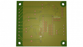
orse. Not sure why the trace thickness need increasing. They are significantly larger than the signal requires.
From my own experience, the sound from the TDA1541 will be better if you use thicker traces from the output pins. Dont belive me.. do two boards, one with thin and one with thick traces. Tell me which sounds better...
But anyway its your board, do as you wish. I thought you were asking for suggestions.
Latest
Here is the latest. It was a bit more involved than I thought, but I think it is better now. I increased audio out trace width. It's now as big as practical I think, and my only point was that electrically, the trace was thick, but could be thicker. Here we go.
Here is the latest. It was a bit more involved than I thought, but I think it is better now. I increased audio out trace width. It's now as big as practical I think, and my only point was that electrically, the trace was thick, but could be thicker. Here we go.
Attachments
I increased audio out trace width.
looks good.
- Status
- This old topic is closed. If you want to reopen this topic, contact a moderator using the "Report Post" button.
- Home
- Source & Line
- Digital Line Level
- Any good TDA1541A DAC kit?