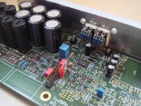
The caps at the drivers were planned like this.
The LED stacking was a correction, because my original clamping at the intput of the IR20957 was slowing down the comparator in a catastrophic way.
I intended to clamp with zener 4V7, but the diode capacities slowed down the comp to bad. The comp out can deliver 15mA and it still took 200ns to charge the diode. So I build the same clamping I used on my earlier breadboard trial, a 5V with 3 LEDs and clamp now with an ordinary 1N4148 against the 5V and a BAS85 against GND. Sloping of the comparator is now around 50ns. Propagation delay also around 50ns. Of course that's not fast, but fast enough and fits to my earlier comparator breadboard. The focus on the comp design is on the jitter noise.
...triangle generator and PWM-comparator running.
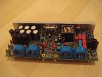
Rail E-caps, fuses, snubbers....
The way of placing the snubbers is not suited for mass production,
but in DIY, this direct connection is easy to implement and easy to adjust to the optimal resonance frequency for optimized snubbering that also covers the headaches of hard switching.
Rail E-caps, fuses, snubbers....
The way of placing the snubbers is not suited for mass production,
but in DIY, this direct connection is easy to implement and easy to adjust to the optimal resonance frequency for optimized snubbering that also covers the headaches of hard switching.
Attachments
Last edited:
Kaspar Sinding Meyer, dead?
Great stuff Choco.
Was thinking to investigate the use of better virtual AC ground in self oscillating designs .... but in many designs this is probably not necessary as it is already implemented by the integrator.
Just googled Kaspar Sinding Meyer (Sovadk here on DIY), to find some of his papers (as referred above).... and find this death announcement...
Kaspar Sinding Meyer : Dødsfald - Berlingske Media - Denmark
Hope I'm wrong …. But how many Kaspar Sinding Meyer’s can there be?
Didn't know him directly, but his brilliant work and always sharing mentality, get you to think he was a really good and decent guy.
What a waste
Sorry to sidetrack the subject …
Kind regards Baldin
@Adam:
Current ripple in the filter chokes runs -/+ 3.75A peak.
This translates to an e-cap ripple current of 1.53Arms.
The Frolyt ERY 470uF/100V is specified for 1A at 100kHz.
With three of them in parallel we are far inside the SOA, even when we consider an imbalance in the current sharing.
@Baldin:
Here the link to the paper of Kaspar Sinding Meyer of my references.
Academia.edu | Minimizing distortion in self-oscillating switching amplifiers | Kaspar Meyer
I am not sure if he is our Sovadk, also not sure about your link.
In any case your link is pointing to a tragedy of a young guy.
In Memorial
http://www.dtu.dk/centre/ele/English/education/phd_students.aspx
I did not have contact to him in the past, but now I started to read more&more about him and feel really sad that he passed away.
Let's give this thread a one week rest in memorial to Kaspar Sinding Meyer.
http://www.dtu.dk/centre/ele/English/education/phd_students.aspx
I did not have contact to him in the past, but now I started to read more&more about him and feel really sad that he passed away.
Let's give this thread a one week rest in memorial to Kaspar Sinding Meyer.
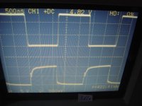
Adjustment of gate drive, dead time and snubbers is always an ongoing process.
Here some screen shots of a preliminary, but typical adjustment with a small overlap. All screen shots of this posting are showing the situation in idling situation. Screen shots during hard switching coming soon.
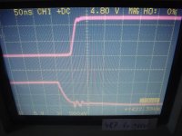
Picture 1: Uce and Ugs of lower MosFet, time base 500ns/Grid
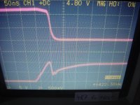
Picture 2: Zoom during turning ON the lower MosFet, time base 50ns/Grid
Picture 3: Zoom during turning OFF the lower MosFet, time base 50ns/Grid
Upper trace: Uce, 50V/Grid (10:1 probe)
Lower trace: Ugs, 5V/Grid (10:1 probe)
Here some screen shots of a preliminary, but typical adjustment with a small overlap. All screen shots of this posting are showing the situation in idling situation. Screen shots during hard switching coming soon.
Picture 1: Uce and Ugs of lower MosFet, time base 500ns/Grid
Picture 2: Zoom during turning ON the lower MosFet, time base 50ns/Grid
Picture 3: Zoom during turning OFF the lower MosFet, time base 50ns/Grid
Upper trace: Uce, 50V/Grid (10:1 probe)
Lower trace: Ugs, 5V/Grid (10:1 probe)
Attachments
A very simple method to examine the details of hard switching is to give zero input signal and connect a load from the amp output to the positive rail and measure on the lower MosFet.
The shown screen shots of the hard switching situation are with 4R7 between amp output and +60V rail.
The load resistor must be a high power device because during the test it will dissipate Vrail^2/R.
Also during hard switching, there should not happen much uncontrolled ringing. This is mostly a question of layout and snubbering.
Picture 1: Zoom during turning ON the lower MosFet, time base 50ns/Grid
Picture 2: Zoom during turning OFF the lower MosFet, time base 50ns/Grid
Upper trace: Uce, 50V/Grid (10:1 probe)
Lower trace: Ugs, 5V/Grid (10:1 probe)
Attachments
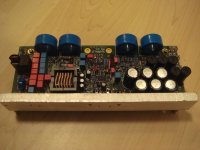
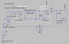
The four large blue torroids are optional common mode EMI filters.
Chosen Material: Ferrite, Epcos T38
Number of turns to be chosen identical on all torroids. Typically in the range between 1 to 3.
First torroid: All supply wires including power GND
Second torroid: Synchronizing signal for multi chanel operation and/or sync with PSU, including sync GND
Third torroid: Audio signal input including signal GND
Fourth torroid: Speaker output including speaker GND
...all these surroundings like the EMI torroids, fuses and protections add complexity and size, but I wanted to have this build not just as a prove of concept. It is intended to become part of my home listening system.
Well, in bridged configuration with 1400W/4R it is sort of overkill, most likely I will use it unbridged.
It took me some time to adjust all parameters in a harmonic balanced way.
...the next few postings shall give a brief overview of the status of today. I feel that this close to the best achievable optimization according my personal taste, but of course further small improvements may evolve with time.
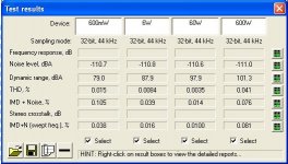
Noise:
My measurement of the idling noise shows 78uVrms wide band noise.
Means with my speakers there is no noise audible at at all.
When I plugged my headphones directly to the amp output, I had to go into a silent room until my ears were able to take notice.
During building the amp I asked myself, which devil inside my soul had pushed me to go for discrete low jitter comparators, fortunately it seems to be worth the efforts.
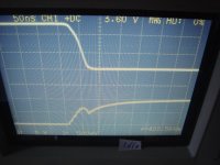
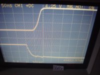
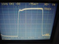
Reproduction of rectangles and driving different impedances:
The first screen shot is showing a +/-15V (10:1 probe) rectangle with 2R load. Sloping time is 4.6us.
The second screen shot is showing again a +/-15V rectangle, but now without load. Sloping time is 4.3us.
...the next few postings shall give a brief overview of the status of today. I feel that this close to the best achievable optimization according my personal taste, but of course further small improvements may evolve with time.
Noise:
My measurement of the idling noise shows 78uVrms wide band noise.
Means with my speakers there is no noise audible at at all.
When I plugged my headphones directly to the amp output, I had to go into a silent room until my ears were able to take notice.
During building the amp I asked myself, which devil inside my soul had pushed me to go for discrete low jitter comparators, fortunately it seems to be worth the efforts.
Reproduction of rectangles and driving different impedances:
The first screen shot is showing a +/-15V (10:1 probe) rectangle with 2R load. Sloping time is 4.6us.
The second screen shot is showing again a +/-15V rectangle, but now without load. Sloping time is 4.3us.
Attachments
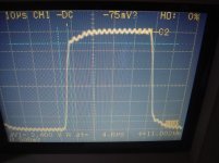
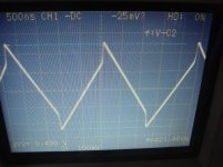
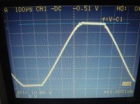
I am using a step shifted triangle, which is giving a good trade off between overall linearity and carrier aliasing.
The first screen shot is showing the step shifted triangle.
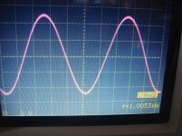
The second screen shot is showing a clean 600W sinewave, without ugly aliasing.
The third screen shot is showing the clipping behavior at 54Vp into 2R. ==> 729W.
You can see that carrier aliasing is starting around 600W. Clipping recovery is fine.
All measurements with 10:1 probes, so the voltages in the screen have to be multiplied by factor 10, in order to read the voltages.
The first screen shot is showing the step shifted triangle.
The second screen shot is showing a clean 600W sinewave, without ugly aliasing.
The third screen shot is showing the clipping behavior at 54Vp into 2R. ==> 729W.
You can see that carrier aliasing is starting around 600W. Clipping recovery is fine.
All measurements with 10:1 probes, so the voltages in the screen have to be multiplied by factor 10, in order to read the voltages.
Attachments
As power supply I am using the hypex SMPS1200.
In order to perform a worst case PSRR measurement I am loading the supply just between one rail and ground in order to generate max imbalance.
(Note: This hypex SMPS has synchronous rectifiers, which keeps imbalance reasonably low even under asymmetric load.)
In the above configuration the PSRR of the 100Hz rail ripple is 68db.

- Status
- This old topic is closed. If you want to reopen this topic, contact a moderator using the "Report Post" button.
- Home
- Amplifiers
- Class D
- System_D_MD, Class D is like chocolate