lemniscate
Hi Damir,
Nothing wrong with his approach. The basic principle is sound. The only thing that's wrong is his example/implementation. Forget that one, but don't forget the lemniscate trick.
Cheers,
E.
Hi Edmond,
But I think that something is wrong with this approach, the current though the cap is not even close to the current trough the emitter resistor. Were is power line current??
Damir
Hi Damir,
Nothing wrong with his approach. The basic principle is sound. The only thing that's wrong is his example/implementation. Forget that one, but don't forget the lemniscate trick.
Cheers,
E.
... but how to place the emitter traces of the output transistors on top of (or underneath) the collector traces I am out of ideas. Is that so impotant as emitter currents are low distortion music signals???
Damir
This is where you need the second layer of the board. The return track can be laid out directly on top of the power track. So the current starts from the centre and runs out to the output transistor collectors, comes out the emitters and thru the emitter resistors into the output trace that return to the middle. Should even be possible to use the emitter resistor to mostly compensate for the collector to emitter offset that Edmond noted in an earlier post to me - #876 .
I haven't done a layout with thermal trak diodes yet but it should still work.
I will post a layout as soon as I can. I have the RS PCB layout software (DSpark PCB) now but I am still not familiar with it so it will take me a while. It looks fairly powerful but with the inevitable complications. I think this could be the LTSpice of PCB layout software.
Best wishes
David
Last edited:
Hello Damir,
My take on the Lemniscrat trick is attached , the current in the paths highlighted travel in opposite direction and the tracks are close together reducing the loop area.
Arthur
Hi Arthur,
Thanks for your help. I think, after careful reading, I understand it better. Important think is in the inductances toward PSU. Abowe 1.5kHz the current flows as Charry says, but bellow it flows inthe lines toward PSU, look blue arrows.
Damir
Attachments
Hi David,This is where you need the second layer of the board. The return track can be laid out directly on top of the power track. So the current starts from the centre and runs out to the output transistor collectors, comes out the emitters and thru the emitter resistors into the output trace that return to the middle. Should even be possible to use the emitter resistor to mostly compensate for the collector to emitter offset that Edmond noted in an earlier post to me - #876 .
I haven't done a layout with thermal trak diodes yet but it should still work.
I will post a layout as soon as I can. I have the RS PCB layout software (DSpark PCB) now but I am still not familiar with it so it will take me a while. It looks fairly powerful but with the inevitable complications. I think this could be the LTSpice of PCB layout software.
Best wishes
David
I don't like double layer PCB with trough the hole metalization, not easy to unsolder at all in case you need to change the componet and that happend more offten then I like.
Maybe without metalization??
I am very interested in your layout, waiting to show it to us.
BR Damir
Isn't the lemniscate trick like a 2-turn air toroid?
No. It's like a 0 turn toroid ie. no toroid at all, that's the point. The second turn unwinds the first turn.
Best wishes
David
Hi David,
I don't like double layer PCB with trough the hole metalization, not easy to unsolder at all in case you need to change the componet and that happend more offten then I like.
Maybe without metalization??
I am very interested in your layout, waiting to show it to us.
BR Damir
I don't think you need thru hole metalization, only essential is 2 layers. Details up to you. I haven't decided about this yet for myself. May depend on details like how the Thermal trak diodes can be worked in to the layout. I share some concerns about difficulties with rework.
Best wishes
David
Hello Damir,
My take on the Lemniscrat trick is attached , the current in the paths highlighted travel in opposite direction and the tracks are close together reducing the loop area.
Arthur
I consider this as just ordinary current cancellation. A lemniscate is a shape like an 8. So one loop can cancel the other.
Best wishes
David
Hi David,
The performance of the super TIS does not rely on high impedance loads. The low THD is achieved by removing nonlinear impedances: Cob and Early effect. Consequently, as there are no other loads involved, the output impedance of the TIS becomes indeed extreme high, tens of MOhms. But, as it appeared, we don't need this. I've simmed the circuit again, this time with a (linear!) load of 100k respectively 100pF and guess what? THD20k was still below 1ppm. So, don't worry.")
I was concerned because I plan to use a BJT OPS and way back at Post #104 you said the front end was not really suitable for that. Presumably the difference between the linear load of 100k and the non-linear load from a BJT triple.
I have considered a BJT triple with a diamond buffer and will sim that at some point.
Best wishes
David
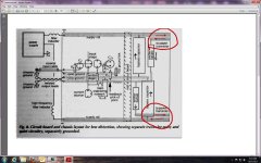
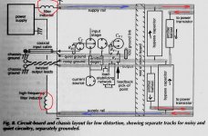
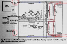
Hello Dave,
To the right of this diagram these two tracks connect to wires which are formed to figure eight and lead to the output devices this is (I think) the lemniscrate trick. The original amp in this article mounted the output devices away from the PCB.
My reading of the input inductor (L) in combination with the C(500uf) and R(for damping) makes 2nd order low pass filter which is used to filter off all high frequency harmonics 1.5Khz and above.
Regards
Arthur
Last edited:
I consider this as just ordinary current cancellation. A lemniscate is a shape like an 8. So one loop can cancel the other.
Best wishes
David
Yes,it is, but only above 1.5 kHz.
Damir
Attachments
Hello Dave,
To the right of this diagram these two tracks connect to wires which are formed to figure eight and lead to the output devices this is I think the lemniscrate trick (I think).
OK, I may have misunderstood what you meant. The emitter resistors and bypass capacitors connections do form a lemniscate shape - but the currents are quite different and so will not cancel well.
Best wishes
David
Hi Dado - Crossed posts but same idea.
Hey Arthur - do you wake up like me and find the "other hemisphere people" have written 60 posts while it was dark in Australia and you missed all the fun?
Last edited:
I don't think you need thru hole metalization
What you guys (David and Dadod) need is a desoldering iron. Like this one. With a proper desoldering iron, through-hole plated boards are actually more robust to rework; tracks are less likely to lift off the board during rework because they're held on by the plating.
Also do not forget the induced signal in the wires coming back from the output heat sink transistor or diode that is used for thermal feedback information.
For this reason I think it's important to capacitor-bypass the connections to the remote diodes where they connect at the Vbe multiplier. Also probably best to use twisted pair connections rather than running tracks on the board.
What you guys (David and Dadod) need is a desoldering iron. Like this one. With a proper desoldering iron, through-hole plated boards are actually more robust to rework;
And only $400 plus delivery! That is pretty steep for infrequent DIY use when an ordinary iron is about 20 times cheaper, but I still may take the professional route.
Best wishes
David
And only $400 plus delivery! That is pretty steep for infrequent DIY use when an ordinary iron is about 20 times cheaper, but I still may take the professional route.
Best wishes
David
All hobbies require some investment, don't they*? Trust me, a desoldering iron is a revelation if you've never used one before. If you do get one be sure to follow all the care instructions to prevent clogging.
* of course it is easy for me to say that because I have 24/7 access at work so I don't need to invest anything!
Last edited:
- Status
- This old topic is closed. If you want to reopen this topic, contact a moderator using the "Report Post" button.
- Home
- Amplifiers
- Solid State
- Has anyone seen this front-end before?