And Ian just confirmed what difference it makes on his product using those batteries.
To be clear, Ian was referring to the Si570 clock performance when he was mentioning batteries recently.
To be clear, Ian was referring to the Si570 clock performance when he was mentioning batteries recently.
yup, nobody, especially Ian, made claims that there was no improvement left on the clocks, on the contrary, he made it clear its pretty much the main area left for tweaking.
I do like the idea of an isolated datastream to the clock board, to enable cutting the ground connection no matter what your source is. weve mentioned it before
Last edited:
Don't hit me if I ask the question many times arised before ")
Does any PC card (PCI, PCIe) which has I2S output exist?
Then integration something like the Twisted Pear Teleporter with Ian's FIFO can implement the PC dedicated music server with USB->I2S or USB->SPDIF cards lacking and with some sort of the isolation also. IMHO.
All the best
Andrey
Does any PC card (PCI, PCIe) which has I2S output exist?
Then integration something like the Twisted Pear Teleporter with Ian's FIFO can implement the PC dedicated music server with USB->I2S or USB->SPDIF cards lacking and with some sort of the isolation also. IMHO.
All the best
Andrey
none natively, there are a couple cheaper types, not super low jitter, but why this legend that i2s will always sound better persists and people go to these lengths, adding extra circuitry for tx and rx, plus added cable length and as much added cost as the fifo spdif board.... it makes no sense to me, seems counter-productive, particularly given the main advantage i2s has is it hasnt had as many conversions. its simply not built for distances and anything to allow them will add its own jitter.
i2s is not always better, to be better the implementation needs to be very clean and as short as possible, it was never made for cables
i2s is not always better, to be better the implementation needs to be very clean and as short as possible, it was never made for cables
Last edited:
none natively, there are a couple cheaper types, not super low jitter...
I see, there are not any good device yet. (Another project for someone?)
Well, for me that is the distance - the Teleporter can deliver abt 30m - that's good because the main audio server can be in the another room.
(e.g. my CAPSv2 dedicated audio PC is abt 1m from the DAC now but it has the connection about 9m via CAT5 with the main server nevertheless).
I mean if I has some good PC card with I2S out and using some good TX-RX device connected to the FIFO I can go with my main PC as audio server and excluding from the audio chain the CAPSv2 with SOtM-tx USB card and linear Teddy Pardo PSU for it and hope the Ian's FIFO will take care about some added jitter
P.S. there are no need for the fifo spdif board at this case
Andrey
Dear Ian,
Thank you very much for your replies to my questions!
MCLK with MHz of nineties is a big present for ES9018 users!
Doesn't Crystek supply CCHD-950 of 90.3168MHz or 98.304MHz to non-bulk purchase customer?
According to my experience, you need the MCLK higher than 90MHz when you play 352.8 kHz sources without any noise, setting OSF = ON.
Some Japanese users say "jitter reduction = OFF" brings a different result. But, I'm not sure.
Thanks Bunpei, will try those settings.
90.xxx and 98.xxx of CCHD-950 or CCHD957 are not available here in Canada or the States. They might be under developing
.Regards,
Ian
yup, nobody, especially Ian, made claims that there was no improvement left on the clocks, on the contrary, he made it clear its pretty much the main area left for tweaking.
I do like the idea of an isolated datastream to the clock board, to enable cutting the ground connection no matter what your source is. weve mentioned it before
That's really a crazy idea, even isolating the clock board from FIFO board!. I don't know how much improvement is gonna be, but at least, it sounds positive
. Ian
Some additional comment running ESS9018 at synchronized mode with 98.3040 MHz MCLK
6. The BIII DPLL bandwidth was set to lowest when I ran the synchronized mode at 98.3040 MHz, the LOCK LED kept solid on for 3 hours during the test, never lost. All signals connected by u.fl cables. The MCLK cable length was 3”.
7. After running for more half hours, it sounds even better. Si570 turns a bit warm. Icc was around 100mA. That should be the warm up time.
8. Three main issues connected to the close-in phase noise: XO crystal quality itself, 1/f noise of power supply and mechanical vibration. So I suspect good suspension may work to improve the Si570 phase noise performance, but by how much still need to be confirmed.
Ian
Quite a few coding jobs of the MCU FW of the Si570 based clock board were finished. Now I can run my ESS9018 (BIII) at synchronized mode with 98.3040 and 90.3186 MHz MCLK from FIFO and Si570 clock board.
The configuration is almost as same as running sync mode from the dual xo clock board except the MCLK frequencies. It sounds wonderful just as I expected. Now the maximal Fs is confirmed working at up to 390 KHz or bit higher without any problem. MCLK is running at 2048*Fs for both 44.1 KHZ and 48 KHz. Stacking the clock board on top of the FIFO board also tested bit-perfect for 98.xxx MHz MCLK at 384KHz.
Compare with 45.xxx and 49.xxx MHZ, running ESS8018 at SYNC mode by an external MCLK closing to 100 MHz is really a challenge. Here are some comments:
1. MCLK U.FL cable should be as short as possible. Higher quality cable is expected to be better result.
2. The DC input voltage range of the Si570 board is 4-5.5V (6V tested no problem but not recommended). I found with 4V and 5.5V it sounds slightly different. But it’s very hard to tell which one is better. I suspect there is a sweet point of input voltage for ADP151, but I’m not sure what that voltage is.
3. Although the Silabs official document mentioned that Si570 is not quite sensitive to the PSU noise, I found it’s not true, at least for this application. The close-in phase noise performance of Si570 is not as good as CCHD950, 957. So, to compete with them, Si570 need better low noise PSU. Both 1/f noise of PSU and the XO crystal itself contribute to the close-in phase noise. After I bypassed the on board low noise LDO and make the Si570 directly powered by a LiFeP04 3.4V battery cell, ESS9018 sounds better with more details and more liquid.
Si570 is a bit special case. It comes with whole DSPLL circuit but a pure XO. I’ll design a battery manager board later on to make the battery as a standard equipped power supply rather than just a testing configuration.
4. Another discovery is, ESS9081 sounds different for a same 44.1 KHz stream with different MCLK frequencies, for example 45.1584MHz and 90.3168MHz. Hard to tell which one is better, but the sound style is a bit different indeed. I know it’s the internal up-sampling digital filter, different performance for different MCLK.
By taking the advantage of Si570 variable frequency output capability, I designed 4 groups of MCLK and *Fs combination in the Si570 control FW. Group is selectable according to different personal preference, or makes it suitable for different DAC chips. They are:
//Group1:Si570 frequency and *Fs combination for low mclk range
{F112896, 256*FS}, //2 44.1 KHz
{F122880, 256*FS}, //3 48 KHz
{F225792, 256*FS}, //4 88.2 KHz
{F245760, 256*FS}, //5 96 KHz
{F451584, 256*FS}, //6 176.4KHz
{F491520, 256*FS}, //7 192 KHz
{F903168, 256*FS}, //8 352.8KHz
{F983040, 256*FS} //9 384 KHz
// Group2:Si570 frequency and *Fs combination for low mid mclk range
{F225792, 512*FS}, //2 44.1 KHz
{F245760, 512*FS}, //3 48 KHz
{F225792, 256*FS}, //4 88.2 KHz
{F245760, 256*FS}, //5 96 KHz
{F451584, 256*FS}, //6 176.4KHz
{F491520, 256*FS}, //7 192 KHz
{F903168, 256*FS}, //8 352.8KHz
{F983040, 256*FS} //9 384 KHz
// Group3:Si570 frequency and *Fs combination for middle mclk range
{F451584, 1024*FS}, //2 44.1 KHz
{F491520, 1024*FS}, //3 48 KHz
{F451584, 512*FS }, //4 88.2 KHz
{F491520, 512*FS }, //5 96 KHz
{F451584, 256*FS }, //6 176.4KHz
{F491520, 256*FS }, //7 192 KHz
{F903168, 256*FS }, //8 352.8KHz
{F983040, 256*FS } //9 384 KHz
// Group4:Si570 frequency and *Fs combination for high mclk
{F903168, 2048*FS}, //2 44.1 KHz
{F983040, 2048*FS}, //3 48 KHz
{F903168, 1024*FS}, //4 88.2 KHz
{F983040, 1024*FS}, //5 96 KHz
{F903168, 512*FS }, //6 176.4KHz
{F983040, 512*FS }, //7 192 KHz
{F903168, 256*FS }, //8 352.8KHz
{F983040, 256*FS } //9 384 KHz
Group1 is designed for low MCLK frequcncy applications (NOS DACs), group2 is for classical DS DAC while group3,4 are for ESS9018. The selection can be made at any time by holding the on board button, the selected setting will be saved into on board flashing memory as well.
5. More researches to the ESS9018 register settings are needed for getting ‘the last drop of juice’ with SYNC mode and different MCLK frequencies. Different options may suitable for different preference.
Ian
6. The BIII DPLL bandwidth was set to lowest when I ran the synchronized mode at 98.3040 MHz, the LOCK LED kept solid on for 3 hours during the test, never lost. All signals connected by u.fl cables. The MCLK cable length was 3”.
7. After running for more half hours, it sounds even better. Si570 turns a bit warm. Icc was around 100mA. That should be the warm up time.
8. Three main issues connected to the close-in phase noise: XO crystal quality itself, 1/f noise of power supply and mechanical vibration. So I suspect good suspension may work to improve the Si570 phase noise performance, but by how much still need to be confirmed.
Ian
That's really a crazy idea, even isolating the clock board from FIFO board!. I don't know how much improvement is gonna be, but at least, it sounds positive
Ian
well it effectively provides galvanic isolation for all inputs from PC ground, prior to the final reclocking stage, even those using usb->i2s input. Thats why I suggested it (and most likely why glt independently suggested it just now), the possible benefit of being isolated from potential slew-rate induced ripple and simultaneous switching noise from the fifo board itself as we push the speeds up; is an aside.
At this late stage it encompasses all of it, not just isolating from USB ground.
Last edited:
P.S. there are no need for the fifo spdif board at this case
Andrey
no, there isnt lol, but its far more complicated and expensive than a simple glass or high quality optical cable and the spdif board, its irrational trying to make i2s work with added parts when it produces identical results. this is assuming you buy another card for the i2s, though even just the transporter is about the same cost as the spdif, which is more flexible.
just using what you already have; I could understand that
Last edited:
I cant understand the fasination with i2S, it is the audio equiv of i2c, both designed to be a local digital bus on a single PCB. If people want to send signals long distance use a deidicated ethernet interface, or SPDIF, its surprising how many interfaces use manchester based encoding for digital transmission where a seperate clock line is not provided. Of course trying to get a clock signal long distance on its own is throught with problems, hence LVDS and manchester type encoding are frequently used. If the supporters of i2S look around you will see very few digital interfaces designed to go off board (ie some distance)these days that have a seperate clock line (the days of RS 232 are long gone).
ian has provided one a well thought out and proffesionaly implemented solution to your demons (ie Jitter)that I have seen in the DIY community. i2s would cause you much more problems, you would still have to try and recover what was left of the clock, never mind the problems of sending the data long distance.
Again ask yourselve why ALL digital interfaces that go off board these days are manchester based encoded and LVDS.
the fascination has its roots in fact, but as per usual its been blown out of proportion and ignores significant factors. if you are having to actually USE the clock recovered from spdif for the MCK and its fairly local transmission, it makes sense to avoid the extra conversions (this is where the fabled higher jitter comes from) but this assumes a well implemented and LOCAL i2s connection to beat good spdif, this is disregarding the fact that the result is the same here unless you need speeds higher than 192 and/or only have a USB->i2s convertor as source
i2s is far more prone to problems, is more difficult to isolate and when we have such a powerful leveler as we have here, it really makes no sense. Sure if you have to send the data from 20M away and the easiest output is i2s, the transporter (which is basically LVDS marce) is the logical choice, but otherwise just using this rather fantastic spdif board, is the only choice that makes sense IMO.
i2s is far more prone to problems, is more difficult to isolate and when we have such a powerful leveler as we have here, it really makes no sense. Sure if you have to send the data from 20M away and the easiest output is i2s, the transporter (which is basically LVDS marce) is the logical choice, but otherwise just using this rather fantastic spdif board, is the only choice that makes sense IMO.
My guess would be is that the i2s love-fest all started with two ideas:
1) try to alleviate some of the issues of spdif
2) the desire of audiophiles everywhere to take a "less is more" aka minimalist approach and less data transformation and less chips 'in the signal path' can be easily sold as a Good ThingTM
All of these interfaces can be well implemented, though examples of poor implementations are readily found without much effort.
FWIW, +1 from me.qusp said:well it effectively provides galvanic isolation for all inputs from PC ground, prior to the final reclocking stage, even those using usb->i2s input. Thats why I suggested it (and most likely why glt independently suggested it just now), the possible benefit of being isolated from potential slew-rate induced ripple and simultaneous switching noise from the fifo board itself as we push the speeds up; is an aside.
At this late stage it encompasses all of it, not just isolating from USB ground.
Can anyone recommend a DAC for use with the FIFO?
Can I use any cheap optical SPDIF cable and USB->SPDIF converter like this as long as it outputs bit-perfect:
Teralink-X2 Native 24bit/96k USB to SPDIF/I2S Converter | eBay
So... how does the FIFO sound?
Is it a revelation?I have a Buf32s dac currently being fed by spdif from a juli@ card. Several questions:
1) Which is the best option for Ian's various boards?
2) I'm not looking for an expensive option but I would entertain a new clock if worth it from a performance standpoint so again whats the best option?
Btw I'm running a fully minimized cmp/cplay system: 15Mb OS.
1) Which is the best option for Ian's various boards?
2) I'm not looking for an expensive option but I would entertain a new clock if worth it from a performance standpoint so again whats the best option?
Btw I'm running a fully minimized cmp/cplay system: 15Mb OS.
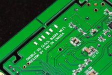
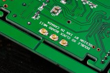
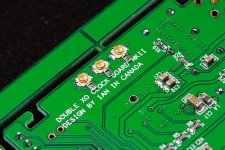
FIFO clock board solutions for dual mono configuration
Somebody ask me how to configure the FIFO and clock board to drive the ESS9018 at dual mono mode. I was not quite sure because I have only one BIII and couldn't confirm it by myself. According to my understanding, a dual mono setup is nothing special, just feeding the same I2S and MCLK signals into two BIII DACs with one set to left and the other to right. So, basically we only need duplicating the I2S and MCLK signals into the two DACs.
Since we already have two u.fl MCLK output sockets on the Dual XO Clock Board, so now there is no any barrier for the clock signals. To duplicate the I2S signals, I think there are two solutions:
1, We already have two I2S outputs on the Dual Xo Clock Board, one from the three u.fl sockets and other from the 7P PH2.0 connector. We can just simply connect them into the two 8018 DACs, everything will be fine. However if we consider similar u.fl cables into the two DACs would be better, the following solution will work for you.
2, Scratching 6 small areas corresponding to the u.fl sockets on green solder mask at the back of PCB, appearing the copper as the u.fl socket ground footprints. Assemble three SMT u.fl sockets with SMT solder station. Connecting I2S signals from the outputs of the flip-flop at top side by flying wires, please don't forget the three 33 ohm impedance matching resistors. Try to make those resistors as close to the FF output as possible. Then, we get two equal groups of u.fl I2S outputs for the dual mono DAC.
I may have to re-layout the PCB of Si570 based clock board one more time, so still get chance to include those u.fl sockets footprint into my design for the optional dual mono applications of ESS9018 and other DACs.
Ian
Attachments
Last edited:
Somebody ask me how to configure the FIFO and clock board to drive the ESS9018 at dual mono mode. I was not quite sure because I have only one BIII and couldn't confirm it by myself. According to my understanding, a dual mono setup is nothing special, just feeding the same I2S and MCLK signals into two BIII DACs with one set to left and the other to right. So, basically we only need duplicating the I2S and MCLK signals into the two DACs.
Since we already have two u.fl MCLK output sockets on the Dual XO Clock Board, so now there is no any barrier for the clock signals. To duplicate the I2S signals, I think there are two solutions:
1, We already have two I2S outputs on the Dual Xo Clock Board, one from the three u.fl sockets and other from the 7P PH2.0 connector. We can just simply connect them into the two 8018 DACs, everything will be fine. However if we consider similar u.fl cables into the two DACs would be better, the following solution will work for you.
2, Scratching 6 small areas corresponding to the u.fl sockets on green solder mask at the back of PCB, appearing the copper as the u.fl socket ground footprints. Assemble three SMT u.fl sockets with SMT solder station. Connecting I2S signals from the outputs of the flip-flop at top side by flying wires, please don't forget the three 33 ohm impedance matching resistors. Try to make those resistors as close to the FF output as possible. Then, we get two equal groups of u.fl I2S outputs for the dual mono DAC.
I may have to re-layout the PCB of Si570 based clock board one more time, so still get chance to include those u.fl sockets footprint into my design for the optional dual mono applications of ESS9018 and other DACs.
Ian
This is great Ian.
Any chance you will modify the dual XO clock board too for GBIII ?
- Home
- Source & Line
- Digital Line Level
- Asynchronous I2S FIFO project, an ultimate weapon to fight the jitter