What about this.
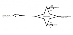
Headphone ground return wire goes directly to audio ground and the left/right SGD are each connected to the audio ground through 10R//100nF.
The audio ground is then directly connectd to regulator/cap multiplier ground.
In my opinion this should be the best solution.
Headphone ground return wire goes directly to audio ground and the left/right SGD are each connected to the audio ground through 10R//100nF.
The audio ground is then directly connectd to regulator/cap multiplier ground.
In my opinion this should be the best solution.
Attachments
Yes, jackinnj introduced the idea in an addendum to your pcb.
One question that another member brought up several posts back. In the matching of pnp to npn, many have told me that it's a pipe dream to get matches that are very close. I know when I refurbed my Adcom 535 amp, I went the distance to match. Finding PNP to NPN matches was darn near impossible. NPN to NPN or PNP to PNP was a piece of cake...the trannies came from the same batch and all matched very closely.
I think the member who asked first said he planned to by 1000 of them, if IIRC.
How close were your matches?
Yes, jackinnj introduced the idea in an addendum to your pcb.
One question that another member brought up several posts back. In the matching of pnp to npn, many have told me that it's a pipe dream to get matches that are very close. I know when I refurbed my Adcom 535 amp, I went the distance to match. Finding PNP to NPN matches was darn near impossible. NPN to NPN or PNP to PNP was a piece of cake...the trannies came from the same batch and all matched very closely.
I think the member who asked first said he planned to by 1000 of them, if IIRC.
How close were your matches?
It isnt obvious but I did spend about 2000 dollars on this project. A lot was trying different transistors for matching. I think you will find these particular transistors will Not take a 1000 to get a match. How close? 5% is what got for the results I published. The jFets - I bought 100 each and found 20 of each matched. Bipolar was easier because the one you will use are closer to being a good compliment in the first place. So, dont panic or worry how it will turn out... I have taken a lot of the cost and drudgery out of it for you (as much as my budget would tolerate, at least). -RNM
Last edited:
Thanks for the additional details. I bought 8 pcs. of the p-fet and then started to think...that ain't gonna do it!
I did find the jfets at Futurelec for about 10 cents each. I bought about 40 of each, so I'm hoping to get in the neighborhood.
BJTs are all USA made, so that should do the trick and get good results.
I did find the jfets at Futurelec for about 10 cents each. I bought about 40 of each, so I'm hoping to get in the neighborhood.
BJTs are all USA made, so that should do the trick and get good results.
Not so easy to get complements...
Not so easy, I'm afraid!! I am the one that post before regarding the problems with MJE200/210. I bought 100 of each and NOT even one pair!
Now I will try with Onsemi (the other where Fairchild's). I will report later on the results. I hope (well better say PRAY) this time will have better luck...
Javier
It isnt obvious but I did spend about 2000 dollars on this project. A lot was trying different transistors for matching. I think you will find these particular transistors will Not take a 1000 to get a match. How close? 5% is what got for the results I published. The jFets - I bought 100 each and found 20 of each matched. Bipolar was easier because the one you will use are closer to being a good compliment in the first place. So, dont panic or worry how it will turn out... I have taken a lot of the cost and drudgery out of it for you (as much as my budget would tolerate, at least). -RNM
Not so easy, I'm afraid!! I am the one that post before regarding the problems with MJE200/210. I bought 100 of each and NOT even one pair!
Now I will try with Onsemi (the other where Fairchild's). I will report later on the results. I hope (well better say PRAY) this time will have better luck...
Javier
Well that must be frustrating! What tests are you matching for?? And, what brand and source did you use?Not so easy, I'm afraid!! I am the one that post before regarding the problems with MJE200/210. I bought 100 of each and NOT even one pair!
Now I will try with Onsemi (the other where Fairchild's). I will report later on the results. I hope (well better say PRAY) this time will have better luck...
Javier
Well that must be frustrating! What tests are you matching for?? And, what brand and source did you use?
Yes indeed, quite frustrating.
As I said in my previous post, I tested them using a Peak Atlas DCA55. They have perfectly equal Vbe, but Hfe was a whole different story:
- MJE200: From 140 to 170
- MJE210: From 210 to 225
I bought them from a reputable (well I think so...) source like Mouser and they are from a reputable manufacturer (again, I think so...) like Fairchild.
This time I will try with On Semiconductor. I will tell you later on the result.
Javier
Good that the Vbe match as compliments. Isnt so important that the Hfe match as the configuration and the fact they are used as followers reduces the matter. use them. Match the fets and the to92 devices for Hfe and Vbe... did those test ok for you?
I'll have matching results this week on the jfets I purchased. I'm still putting together the order with Mouser and have mostly picked On Semi for this build.
Someone bought up all of what they had on stock for one of the OnSemi transistors, but they refilled inventory asap with several thousands. I think it was the 2N5088G.
Someone bought up all of what they had on stock for one of the OnSemi transistors, but they refilled inventory asap with several thousands. I think it was the 2N5088G.
about having ground plane
I have been researching a lot about ground loops and come across digital and analog plain ground in a single pcb.one way to accomplish it is having a two ground returns for analog and digital. but this two ground plane should meet at one point in pcb and having one return gnd..having two returns for this two ground going to star gnd,,,,pcb will act like a dipole antenna and will attract more noise.
I am not an engineer but this confuse me...and needs a lot of understanding.
regards,
joel
p.s.
I have been studying your layout and want to know if you intended to separate the power gnd and signal making sure that it does not cross each other boundary.
No. Thats fine. can also put a bypass cap across the 10 ohms so the ground is low at Hf and only affective at 'hum' frequencies.
Also can try using shunt caps, as shown on pcb, withOUT lowest esr for damping, if needed.
I have been researching a lot about ground loops and come across digital and analog plain ground in a single pcb.one way to accomplish it is having a two ground returns for analog and digital. but this two ground plane should meet at one point in pcb and having one return gnd..having two returns for this two ground going to star gnd,,,,pcb will act like a dipole antenna and will attract more noise.
I am not an engineer but this confuse me...and needs a lot of understanding.
regards,
joel
p.s.
I have been studying your layout and want to know if you intended to separate the power gnd and signal making sure that it does not cross each other boundary.
Last edited:
Yes.p.s.
I have been studying your layout and want to know if you intended to separate the power gnd and signal making sure that it does not cross each other boundary.
I have been studying your layout and want to know if you intended to separate the power gnd and signal making sure that it does not cross each other boundary.
See his post at http://www.diyaudio.com/forums/head...eadphone-amp-linear-audio-31.html#post3066530
This explains his approach quite well.
Good that the Vbe match as compliments. Isnt so important that the Hfe match as the configuration and the fact they are used as followers reduces the matter. use them. Match the fets and the to92 devices for Hfe and Vbe... did those test ok for you?
Well I just finish testing the rest of semiconductors. This time I have been luckier. I could find good complements for both the 2n5087/5088 (equal Vbe and almost equal Hfe in the range 395 to 420) and JFET 2n5457/5460 (tested using the method you described in Linear Audio article gave me a range of 0.8 to 0.9 in a good bunch of pieces). So, according to your suggestion I could try with the MJE's available, despite not being a perfect match.
Anyway, I will receive the new MJE's from On Semi this week so I hope I may find better complements.
Javier
about grounding..
check this...
http://www.hottconsultants.com/pdf_files/june2001pcd_mixedsignal.pdf
regards,
joel
check this...
http://www.hottconsultants.com/pdf_files/june2001pcd_mixedsignal.pdf
regards,
joel
once again you need to know the frequency dependence - his digital current concentration plot only applies for MHz signal components
the partial mutual inductance Fast Henry sim I posted shows that you're only ~ 1/2 way there by 20 kHz
most Power Supply gnd contamination effects happen at low multiples of the line frequency - your only hope of controlling these currents is by physically restricting the path - discrete pwr/return trace routing - not planes
most audio current effects are also too low for the single plane concept to work
hierarchical gnds, star on star, “clean’, “dirty” paths established by explicit wires, trace geometry, ordering are the audio frequency tools you need
Ott shows how to get these low frequency effects right too - just not emphasized in that link
once again you need to know the frequency dependence - his digital current concentration plot only applies for MHz signal components
the partial mutual inductance Fast Henry sim I posted shows that you're only ~ 1/2 way there by 20 kHz
most Power Supply gnd contamination effects happen at low multiples of the line frequency - your only hope of controlling these currents is by physically restricting the path - discrete pwr/return trace routing - not planes
most audio current effects are also too low for the single plane concept to work
hierarchical gnds, star on star, “clean’, “dirty” paths established by explicit wires, trace geometry, ordering are the audio frequency tools you need
Ott shows how to get these low frequency effects right too - just not emphasized in that link
Dont rule out shielding for use of planes opposite the pcb wires and for low Z at Mhz for stability. -RNM
this bothers me....
Is it ok not to use bridge on those two ground planes?how about the high resistance it would create plus running wires to star gnd.?are these ideas applicable only for mixed analog and digital signal?how about gnd loops are these cause by high resistance?
as what you have said gnd planes are for shield and would be very difficult to separate diff gnd, returns if I use it.
regards,
joel
For perfectionist way -- I always advocate having the power supply reg right at the amp circuit. .. shortest distance from circuit and ditto for the grounds.
Integrate the pwr supply onto the amp pcb is best way. Or, second best, locate the pwr supply pcb right close to the amp pcb.
Last edited:
- Home
- Amplifiers
- Headphone Systems
- Marsh headphone amp from Linear Audio