And yes, I know the VAS might look like "overkill", by actually applying a current mirror and still run a relatively high current of 35mA with almost 200V across. But, it's worth it and it was the only way to have it meet all the functional requirements I wanted the VAS to meet ")
Say.. would you guys want me to draw a simplified functional diagram of the circuit or is it comprehensible as it is?
I've now 'revealed' the near final design but so far I've not noticed any serious comments about it. This makes me doubt myself. Did I in fact create a dud? Is there stuff in the schematic of which you'd say "what moron put that together"? I'm all open to critics both to my perceived knowledge as well as the design. I can handle that
I've now 'revealed' the near final design but so far I've not noticed any serious comments about it. This makes me doubt myself. Did I in fact create a dud? Is there stuff in the schematic of which you'd say "what moron put that together"? I'm all open to critics both to my perceived knowledge as well as the design. I can handle that
the added C "for stability" are odd - not often seen, needed in small signal frontend, VAS - normally only output Q
parts selection seem strange too - a 4 A driver Q biased at 11 mA? - when the VAS itself is running at 30 mA?
the oversize parts have huge nonlinear, parasitic C, are slower than properly sized parts too
and the conceit of all fet while grabbing the popular imagination really doesn't seem like "engineering" to me - when bjt will have better performance at some points in the circuit
Hi guys, thank you for your honest responses
@AKSA: Hugh you inspire me to continue trying to get the most out of this schematic. Personally I'm confident building it, my previous amp worked out really nice too. But since this isn't a small amp I'd like to keep glaring errors to a minimum while still being experimental in design.
@jcx: Yeah it may look like that, but what can I say.. I've noticed that with a small feedback cap over the IPS CCS cascode the overall standing currents in the IPS stage are reduced. It's more quiet. That to me is a hint that the current control otherwise is a bit oscillation prone, most likely due to the IRF610/620's speed a.k.a. high transconductance. HEXfets tend to be a little erratic if not compensated or severely slowed down, they have originally been designed as switching FETs, not so much as lineair operating FETs. Yet they make great cascodes.
The choice for the IRF(9)620 was because these are more quiet than the 610/9610 in the driver position. While the amp output was quit, there was still a bit of regulation oscillation in the driver stage. You may think the device is overkill, but at a 10mA current it's still operating in a lineair fashion, Vds is rather high and reduces its capacitances still. Those capacitances are what makes the stage quiet and stable out, why have faster-than-needed devices in relation to the other stages? It just requires extra compensation. They also have a high transconductance while the increased C acts as free local compensation. Besides, I wanted TO220 devices that can handle 200V breakdown and they fit the bill That's my reasoning for the driver transistors. If you have suggestions for other types you may think have a better result, please don't hold back.
As for using 30mA in the VAS and around 11mA in the driver, that's because the VAS is the most critical part of the voltage output stage. The drivers are source followers and as such are not responsible for creating the voltage swing. Their task is to isolate the OPS from the VAS output rail. The higher VAS current increases linearity and decreases distortion as relatively seen, is impacted less by the minor load, which gets less minor at higher frequencies due to the capacitive load. Even then it still provides the oomph to still successfully regulate a 500KHz input signal with around 0.1% THD. 35mA - 40mA appeared to be the sweetspot for this VAS
As for your comment about all-FET, yeah I would have to agree that BJTs can be better in certain aspects. In the end, every part has its place in a schematic. "All-FET" is more self-applied constraint than it is because everything would be better using FETs. It's just a nice idea that an amp design is fully FET based as a statement that FETs suit the job for all amp parts just as much - albeit with a slightly different thinking, mostly biassing and driving. That doesn't mean I'm shy of using BJTs - there's nothing wrong with modding the design and replace some parts with BJTs. My version however will attempt to use FETs exclusively
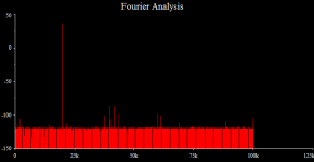
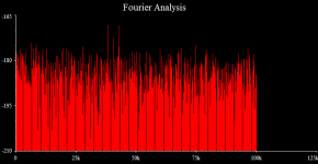
@homemodder: Attached to this post you'll find the THD20 at 500W/4R, the corresponding hi-res FFT and a FFT with the input grounded. And no, I don't design VLSI for a living, although it surely is an appealing field. I'm a software writer by trade, an electronics engineer in my spare time
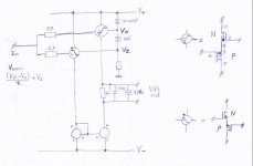
VAS operation
The first image is a picture of how the VAS works. It's actually pretty straight forward. The VAS rail has a top and bottom section. The bottom section is mirrored. This creates two current paths that can be controlled. you'll see that the input controls both current valves. The valves are opposite in action. Since they're differential, the other inputs are tied to a fixed reference. This actually is a nice perc as the valves need to be biassed to set the idle VAS current. The bias voltage between the two 'grounded' valve inputs determines the quiescent current. This can be adjusted by a trimmer if greater accuracy is wanted. The current valves drawn in the schematic are made of a complementairy pair with the sources tied to each other. They can be easily recognized in the original schematic
The huge benefit of this way of controlling the VAS current is that the cut-off behaviour of the valves is much better than VAS gain devices referenced against the supply rail (sources tied to supply rails). This is because the reference is now set at a much lower voltage. This means, that at higher frequencies when more swing appears on the IPS output, that the VAS input will still not clip and can accomodate the higher input swing. This greatly helps with transient response and squarewave performance as the IPS output swing excursion can get quite big. Under normal operation eventhough the valves consist of an N and P fet, they're still class A biassed.
A more elaborate version would mirror the top part of the VAS much like the bottom part and have the mirrored part run to GND. Then, the valve is to be placed in this leg. Because that leg is not responsible for the output swing, the valve can be referenced at any voltage, and thus referenced at the voltage halfway the maximum swing excursion range of the IPS output which lies between Vsat of the top mirror and Vsat of the cascode with maximum positive swing input. This version had slightly better THD numbers, most likely because both the top and bottom end of the VAS were fully symmetric.
Anyways, that's just my way of thinking.. I'm curious about downscaling the amp and see what numbers I would end up with at much lower watts lol
@AKSA: Hugh you inspire me to continue trying to get the most out of this schematic. Personally I'm confident building it, my previous amp worked out really nice too. But since this isn't a small amp I'd like to keep glaring errors to a minimum while still being experimental in design.
@jcx: Yeah it may look like that, but what can I say.. I've noticed that with a small feedback cap over the IPS CCS cascode the overall standing currents in the IPS stage are reduced. It's more quiet. That to me is a hint that the current control otherwise is a bit oscillation prone, most likely due to the IRF610/620's speed a.k.a. high transconductance. HEXfets tend to be a little erratic if not compensated or severely slowed down, they have originally been designed as switching FETs, not so much as lineair operating FETs. Yet they make great cascodes.
The choice for the IRF(9)620 was because these are more quiet than the 610/9610 in the driver position. While the amp output was quit, there was still a bit of regulation oscillation in the driver stage. You may think the device is overkill, but at a 10mA current it's still operating in a lineair fashion, Vds is rather high and reduces its capacitances still. Those capacitances are what makes the stage quiet and stable out, why have faster-than-needed devices in relation to the other stages? It just requires extra compensation. They also have a high transconductance while the increased C acts as free local compensation. Besides, I wanted TO220 devices that can handle 200V breakdown and they fit the bill
That's my reasoning for the driver transistors. If you have suggestions for other types you may think have a better result, please don't hold back.As for using 30mA in the VAS and around 11mA in the driver, that's because the VAS is the most critical part of the voltage output stage. The drivers are source followers and as such are not responsible for creating the voltage swing. Their task is to isolate the OPS from the VAS output rail. The higher VAS current increases linearity and decreases distortion as relatively seen, is impacted less by the minor load, which gets less minor at higher frequencies due to the capacitive load. Even then it still provides the oomph to still successfully regulate a 500KHz input signal with around 0.1% THD. 35mA - 40mA appeared to be the sweetspot for this VAS
As for your comment about all-FET, yeah I would have to agree that BJTs can be better in certain aspects. In the end, every part has its place in a schematic. "All-FET" is more self-applied constraint than it is because everything would be better using FETs. It's just a nice idea that an amp design is fully FET based as a statement that FETs suit the job for all amp parts just as much - albeit with a slightly different thinking, mostly biassing and driving. That doesn't mean I'm shy of using BJTs - there's nothing wrong with modding the design and replace some parts with BJTs. My version however will attempt to use FETs exclusively
@homemodder: Attached to this post you'll find the THD20 at 500W/4R, the corresponding hi-res FFT and a FFT with the input grounded. And no, I don't design VLSI for a living, although it surely is an appealing field. I'm a software writer by trade, an electronics engineer in my spare time
VAS operation
The first image is a picture of how the VAS works. It's actually pretty straight forward. The VAS rail has a top and bottom section. The bottom section is mirrored. This creates two current paths that can be controlled. you'll see that the input controls both current valves. The valves are opposite in action. Since they're differential, the other inputs are tied to a fixed reference. This actually is a nice perc as the valves need to be biassed to set the idle VAS current. The bias voltage between the two 'grounded' valve inputs determines the quiescent current. This can be adjusted by a trimmer if greater accuracy is wanted. The current valves drawn in the schematic are made of a complementairy pair with the sources tied to each other. They can be easily recognized in the original schematic
The huge benefit of this way of controlling the VAS current is that the cut-off behaviour of the valves is much better than VAS gain devices referenced against the supply rail (sources tied to supply rails). This is because the reference is now set at a much lower voltage. This means, that at higher frequencies when more swing appears on the IPS output, that the VAS input will still not clip and can accomodate the higher input swing. This greatly helps with transient response and squarewave performance as the IPS output swing excursion can get quite big. Under normal operation eventhough the valves consist of an N and P fet, they're still class A biassed.
A more elaborate version would mirror the top part of the VAS much like the bottom part and have the mirrored part run to GND. Then, the valve is to be placed in this leg. Because that leg is not responsible for the output swing, the valve can be referenced at any voltage, and thus referenced at the voltage halfway the maximum swing excursion range of the IPS output which lies between Vsat of the top mirror and Vsat of the cascode with maximum positive swing input. This version had slightly better THD numbers, most likely because both the top and bottom end of the VAS were fully symmetric.
Anyways, that's just my way of thinking..
I'm curious about downscaling the amp and see what numbers I would end up with at much lower watts lolAttachments
Well, a small update I'm now pretty close to the final version and will start working on the full schematic soon. Reading over posts I noted mr. Cordell mention TIM, IMD and figured I'd add a FFT for this amp with a 19K+20K input signal. It looks promising!
I'm now pretty close to the final version and will start working on the full schematic soon. Reading over posts I noted mr. Cordell mention TIM, IMD and figured I'd add a FFT for this amp with a 19K+20K input signal. It looks promising!Attachments
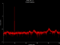
What power level is that? The IMD looks to be almost indistinguishable from the noise.Well, a small update
How about PIMD?
Nice design, its very similar to a australian amp lineup except youve opted for darlington vas and and therefore better THD figures, square wave response looks very good too.
Since the design is built and tested you should present it here as well, there are many DIYers that prefer full symmetrical amps and there practically arent any here shown with full completion and PCB that they could build.
Hi Homemodder, apparently I had looked over this comment. Yeah it might be a good idea to release MF-80 on this forum as well. The amp definitely is a treat to the ears
Frankly since I've hooked it up to do listening tests, it hasn't been disconnected since lol. If there's a MOSFET amp that sounds like it sets the music free, it's gotta be this one! Coupled with a proper set of high-end speakers, closing your eyes places you onto an infinite plane of listening pleasure. No matter whether it's the lows, mids or highs - discernable transparency and definition is omnipresent.
Last edited:
Look above only a few posts.Great to hear that! Can you post some measurements: THD (FFT) and IMD dual tone?
Thx!
That's simulation, for the SOM amp though. For MF-80 I hadn't made images of IM plots.
As for SOM, I'm still not done.. While the basic premise works rather well, I'm still working out ways to reduce the VAS current and associated dissipation without adversely affecting performance. On top of that, I'm also trying to figure out some sort of an autobiassing scheme that allows one to set accurately the VAS current and making it immune to temp drift. Lots of puzzling to be done still
As for SOM, I'm still not done.. While the basic premise works rather well, I'm still working out ways to reduce the VAS current and associated dissipation without adversely affecting performance. On top of that, I'm also trying to figure out some sort of an autobiassing scheme that allows one to set accurately the VAS current and making it immune to temp drift. Lots of puzzling to be done still
Hi, MagicBox
I have a question for you regarding cascodes for input JFETs, Q7 & Q8, ZVN3306A
Did you opt for MOSFET cascodes instead of BJT just because you want an all-FET design or there are also reasons related to sound quality (sounds better with MOSFET than BJT) ? As far as I know Vbe drift with temperature is smaller than Vgs. The effect is probably a small one since we are discussing cascodes devices, but one of the purposes for cascode is to keep Vds for JFETs constant. So in this regard maybe BJT is better than MOSFET.
Also devices type was chosen on purpose or another N-Ch MOSFET like BS170 will do the job as well ?
Regards,
Tibi
Hello fojica,
Yes, that was/is the primary reason for choosing FETs, an all-FET amp. However, BJTs would work alright too. I personally think the difference would be neglible since under normal conditions, power dissipated remains the same with or without signal which would reduce realtime temp fluctuations. On top of that, the cascodes sit rather 'high' on their JFETs (~ 17V Vds), further minimizing Vds modulation. Altogether, I don't think there wouldn't be any notable differences to warrant choosing BJTs specifically in this application, but I may be wrong.
As for device type, I initially used BS170 (and BS250 for the P counter part) but I was told these had become obsolete and so replaced them with the Zetex ones. Any device that has a high transconductance would work fine as long as it would be suitable to operating conditions (voltage/current).
I hope that answers your questions
Last edited:
Hi, MagicBox
Absolutely - and thank you for the answers
I was asking about device type because I also used BS170 & BS250 with good results.
Maybe one day I'll try BJT vs MOSFET as cascode devices to a JFET (same amp) - just curios subjectively on sound, if any difference. Vds for JFET also around 18-20V.
Regards,
Tibi
I have been lurking on this thread since the start, as I have not been able to give any sage advice and I would be the first to admit that the discussions here are way out of my depth although I’m learning... however I am so eager to build and listen. I have PM’ed a few members to try to rouse some interest just so it doesn’t die.
I am willing to offer in other ways such as enclosure engineering or organising circuit board group purchases
Apologies for the non-contributory content....
Snax
I am willing to offer in other ways such as enclosure engineering or organising circuit board group purchases
Apologies for the non-contributory content....
Snax
- Status
- This old topic is closed. If you want to reopen this topic, contact a moderator using the "Report Post" button.
- Home
- Amplifiers
- Solid State
- "State-Of-MOS": 200W Ultra Low Distortion Pure FET Amplifier