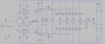
Doing some simulation with a complementary JFET input stage using 2SK246/2SJ103, instead of the usually recommended 2SK170/2SJ74 JFETs.
Mostly for fun and to see what I could get out of it.
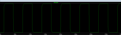
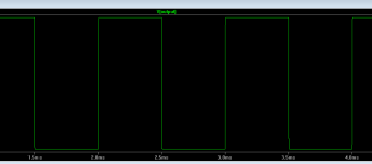
Was a little amazed at the insane slewrate I could achieve and still maintain a nice looking 20 KHz squarewave and good phase and gain margins.
Only downside is THD-20 that is around 0.02% at 60 Watt, 8 Ohm load, the 1 W 8 Ohm load THD-20 is a more decent 0.001XXX%.
THD-1 1 W, 8 Ohm load is 0.0002XXX% rising to 0.0017XX% at 60 W, 8 Ohm load.
Mostly for fun and to see what I could get out of it.
Was a little amazed at the insane slewrate I could achieve and still maintain a nice looking 20 KHz squarewave and good phase and gain margins.
Only downside is THD-20 that is around 0.02% at 60 Watt, 8 Ohm load, the 1 W 8 Ohm load THD-20 is a more decent 0.001XXX%.
THD-1 1 W, 8 Ohm load is 0.0002XXX% rising to 0.0017XX% at 60 W, 8 Ohm load.
Attachments
Last edited:
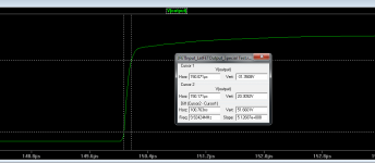
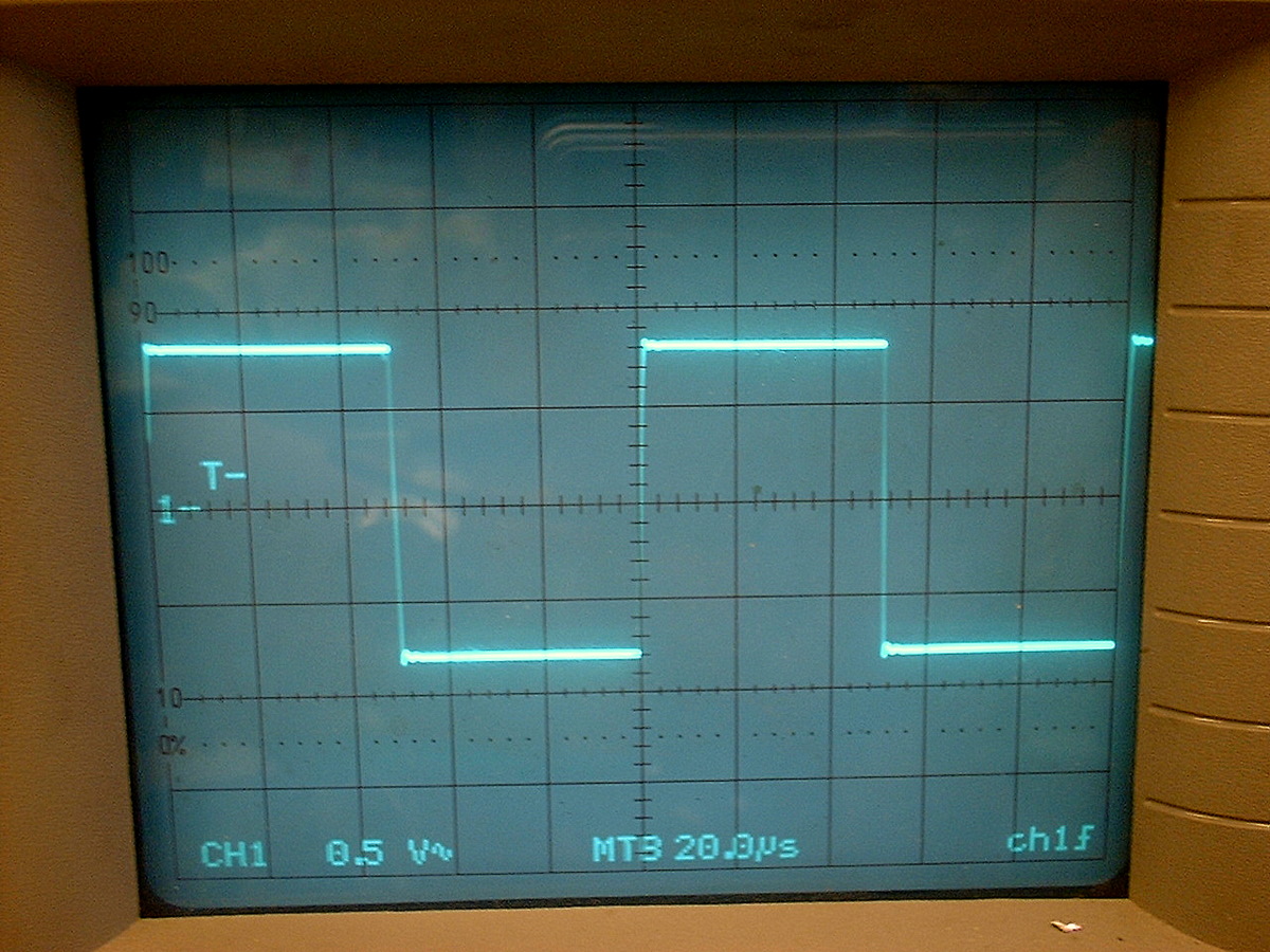
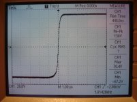
To measure the slew rate of an amplifier you measure the rise and fall times of a pulse waveform. Rise time is measured from 10% above the minimum voltage to 90% of the maximum voltage and fall time is measured from 10% below the maximum voltage to 90% of the minimum voltage. If you are measuring a square wave output of an amplifier the 10 and 90% points should be of equal voltage and opposite polarity
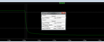
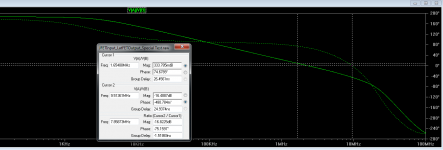
The rising slew rate that you measured in your first post (pic #2) was between -31.33 and 20.3 Volts and the falling slew rate (pic #3) were between 33.97 and -16.11 Volts.
It’s easy to get insane slew rates when you throw out the slower parts of the signal.
The rising slew rate that you measured in your first post (pic #2) was between -31.33 and 20.3 Volts and the falling slew rate (pic #3) were between 33.97 and -16.11 Volts.
It’s easy to get insane slew rates when you throw out the slower parts of the signal.
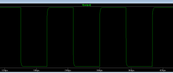
This, as an example is a 10KHz squarewave from an amplifier having a modest ~24V/µs slewrate:I find the 20K waveshape incoherent with that kind of performance: it is much too rounded.
Ah well, it looked too good to be true anyway.
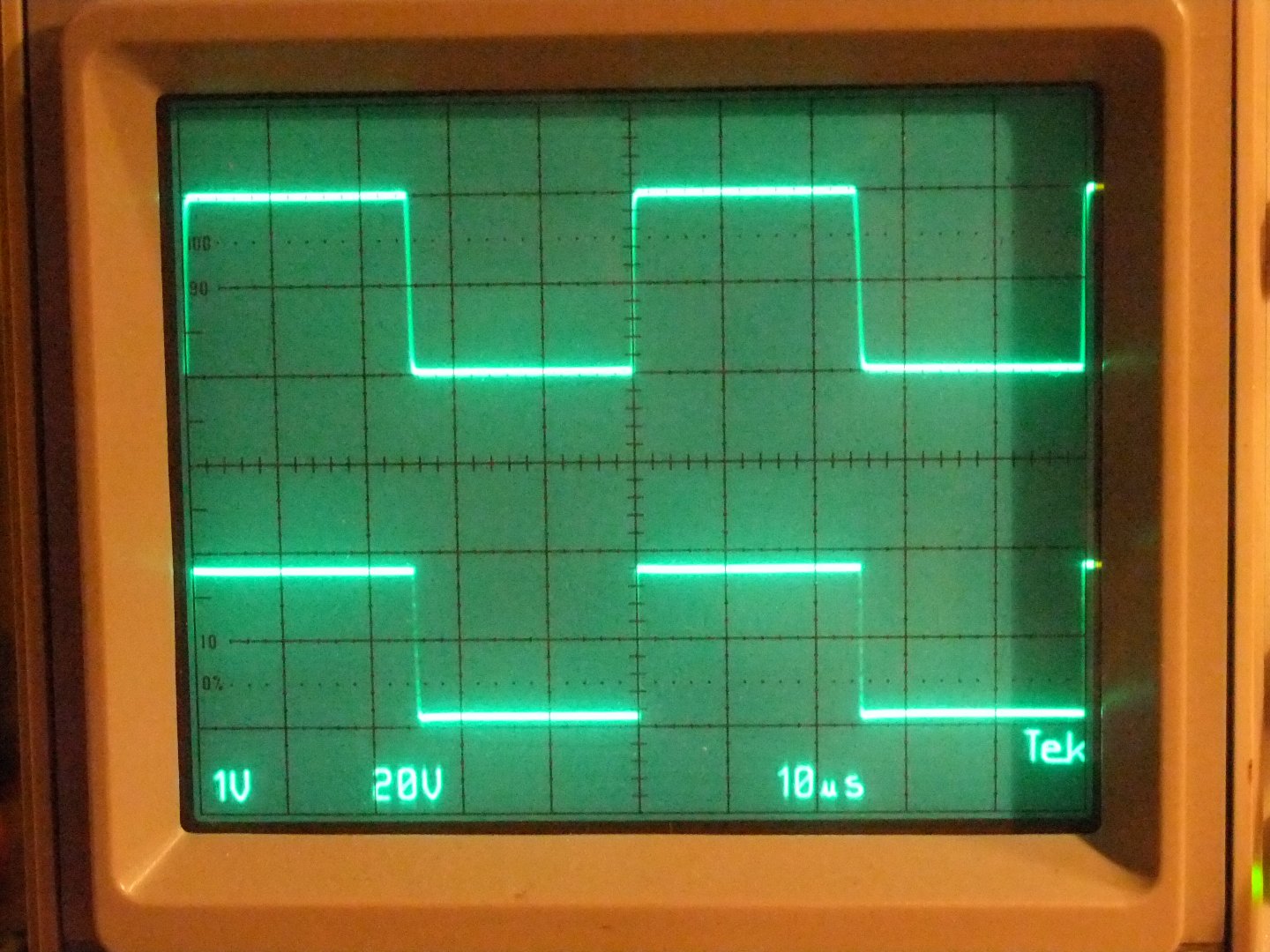
By using the 10%/90% method for determining slewrate I get a number of around 70V/uS.
That was obtained by measuring slewrate between +34V/-34V. Maximum voltage being +38V/-38V.
Which sound a lot more ressonable and plausible.
By using the 10%/90% method for determining slewrate I get a number of around 70V/uS.
That was obtained by measuring slewrate between +34V/-34V. Maximum voltage being +38V/-38V.
Which sound a lot more ressonable and plausible.
The question here is does your simulation in this case represent the real world? 5pf Cdom seems a bit low to me.
Well, it works down very well at 5pF, 4pF is ok, and at 3pF it starts to show some problems and without any Cdom it just goes crazy into oscillation.
SSA amp measured slew rate 250V/us
Impressive.
A great issue by simulation are the not present parasitic components from real world. An example is the capacitor parallel to the NFB resistor, that is connected between tje output and the inverted input. By various commercial amps this capacitor exist not as a component, but neverthless this capatitor is present (in the aera between 10pF and 50pF, independend from the posotion of the copper-wires from the PCB).The question here is does your simulation in this case represent the real world? 5pf Cdom seems a bit low to me.
By a power amp example from the German brand MERACUS, that I have get for re-design (causes unwanted oscillation), I measure a value about 30pF.
This means for me, in the circuit for simulation one must actually introduce all values for existing virtual capacitors and inductors, which result from the PCB trace routing (at least the most important parasitic devices).
Unfortunately a great challenge.
Because most engineers does that, CAD for audio amps has a very bad call - see various comments towards the end about
http://www.diyaudio.com/forums/solid-state/89023-bob-cordell-interview-error-correction.html
Last edited:
I tried WikiP, but I did not find it.
Taking the slew rate time period at 90% of the signal change, rings a bell.
Could it be from 5% to 95%, i.e. 90% of the whole signal change or as stated earlier 10% to 90% for an effective 80% of the whole signal change.
Can some/many confirm?
Taking the slew rate time period at 90% of the signal change, rings a bell.
Could it be from 5% to 95%, i.e. 90% of the whole signal change or as stated earlier 10% to 90% for an effective 80% of the whole signal change.
Can some/many confirm?
Andrew, scroll down to figure 4.
Slew Rate
More,
http://ece.wpi.edu/~mcneill/handouts/RiseTimeMeasurement.pdf
http://www.interfacebus.com/IC_Output_Slew_Rate.html
http://www.falco-systems.com/high_voltage_amplifiers.html
Although, Jim Williams says the middle 2/3.
http://cds.linear.com/docs/Application Note/an94f.pdf
Slew Rate
More,
http://ece.wpi.edu/~mcneill/handouts/RiseTimeMeasurement.pdf
http://www.interfacebus.com/IC_Output_Slew_Rate.html
http://www.falco-systems.com/high_voltage_amplifiers.html
Although, Jim Williams says the middle 2/3.
http://cds.linear.com/docs/Application Note/an94f.pdf
Last edited:
I think Tektronix measuring equipment company knows something about this simple question. ")
Look to my Tek plot of 1 kHz square wave and you will see that it starts to measure slew rate from 10% to 90% of the signal Vpp (rise time). Also you can readout the same value from the plot itself or from the right side value result (80% of 138Vpp in 448ns rise time).
Look to my Tek plot of 1 kHz square wave and you will see that it starts to measure slew rate from 10% to 90% of the signal Vpp (rise time). Also you can readout the same value from the plot itself or from the right side value result (80% of 138Vpp in 448ns rise time).
Last edited:
- Status
- This old topic is closed. If you want to reopen this topic, contact a moderator using the "Report Post" button.
- Home
- Amplifiers
- Solid State
- 500v/uS slewrate, really?