Sorry but wich version
In fact the voltage for Vin divided by the curent of the DAC
give us less than 1 ohm
Perhaps we have make a mistake
Hope not but I am using this one:
Take the p-p V plot of Vin and divide by the p-p current deliver, I'm getting 20 ohms. Tried a few different types of current sources (ie the one in the photo and a current source with 1.5k resistor in series to simulate a typical dac output impedance.) Both came up with 20 ohms.
Btw, This is the most exciting DAC analog stage I have ever seen. But I know first hand that input ipedance needs to be at least under 5 ohms for most of the older DAC's to have te lowest distortion with -60dB signals.
One other thing we need to figure out is how to deal with the 2mA offset of the TDA1541.
I do not want to seem rude but imho that last circuit just looks like the common opamp iv with its implications only with tubes why have you given up on transconductans ivs?
I believe they are the same topology really, the one I posted I think was the first version, then the 6F12P was replaced with the Mofset.
Chanmix mentioned the all tube 6F12P version as being so similiar to the hybrid as to not be audibly different, but I'm getting a much higher input impedance on the sim than he reports.
I like the 6F12P version because it seems easier to integrate with the TDA1541, which wants to see 0VDC on its output and it draws 2ma of current (offset).
But this is exciting stuff, biggest development in IV I've seen. Never was a fan of the "simple" feedback free BJT idea, BJT's are just not linear enough for no NFB operation, and all the NFB with them configured in an opamp makes them have terrible input impedance behavior with the square wave outputs from DAC's. This "super common gate" topology is groundbreaking stuff.
Just got to get it to the point where we have less than 5 ohms input impedance (broadband), source the 2mA offset at 0VDC, and DC couple the ouput then we have the TDA1541 analog stage we've all been looking for

As is the 6F12P version looks perfect for an AD1862/5 project.
The circuits in 36 and 41 are topologically different.
In the circuit in post 36 the Mosfet creates a feedback loop with the tube thus lowering the impedance as seen from the dac. The mosfet does not (and can not) have linear gain over frequency hence the impedance as seen from the dac will rise with increasing frequency this is not ideal as a dac outputs square steps (lot of HF content much much higher than the audio band). But the I/V is still a transconductance stage.
The circuit in post 42 I view as a discrete opamp. U1 senses the voltage difference between K1 and G1 (as would the differential input of an opamp). This error signal is used to drive U2 to cancel out the voltage difference by driving its cathode to zero out the voltage by forcing current through the IV resistor R1 (as would the output of an opamp do)
Since U1 also has a current source load I would guess the open loop gain of the circuit to also be similar to that of an opamp ( ie gain dropping of with increasing frequency).
Hi Regal & Tazzz
The scheme of Regal is nearest my first version of IVTCY
indomptable version in fact , with Chanmix & Yves07 we work
on the "super common gate" project to go more in detail
This following capture is my actual version , full tube, with
a notch filter around 44.1 Khz
my power supply is the second (rev 2) in the zip file
the IVCTY the "rev2g alain93" also in the zip file
I listen it every day in reality without any problem
I forgot, for the input impedance the curve is the "U"
Enjoy
Attachments
Last edited:
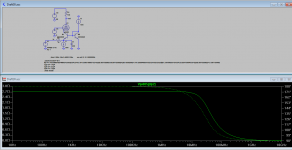
Oh ... The schematic you are working on is quite old, the current source on the pentode's anode led to too much instability.
Here is a even more simplified version, the input impedance as seen by the TDA1543 is less than 0.1Ω


This can work with the full tube version. Give it a try with a TDA1543, it's cheap and the result is ... surprising
greg
Here is a even more simplified version, the input impedance as seen by the TDA1543 is less than 0.1Ω
This can work with the full tube version. Give it a try with a TDA1543, it's cheap and the result is ... surprising
greg

Hi Tazzz
Your input impedance is too big in front of a simple AOP
What's your voltage for Vin
For the model of DAC look at ours scheme, the version voltage generator and
resistor is less accuracy than a current generator drive by a voltage generator
In mind we prefer for the input impedance a rising edge for low frequency
to prevent 50 hz disturbing
Hi Tazzz
Your input impedance is too big in front of a simple AOP
If I'm not blind the input impedance of my circuit is about half of the one you posted from 10Hz and up and its very linear with frequency.
What's your voltage for Vin
For the model of DAC look at ours scheme, the version voltage generator and
resistor is less accuracy than a current generator drive by a voltage generator
The voltage at Vin (the bjts emitter, what the dac would see ) is close to 0V DC and AC at 1Khz is +/-6mV. Most dacs are poor current sources having an output impedance in the region of 1Khom or so. So a voltage source + resistor is a good model.
I used 4mA P-P and 1500R I/V for 2VRms fullscale.
If I'm not blind the input impedance of my circuit is about half of the one you posted from 10Hz and up and its very linear with frequency.
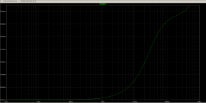
Hi Tazzz, I don't get it. The bode diagramm above shows the input impedance being lower than 0.1Ω from 8Hz to 250kHz. This is pretty much 30x less than the graph you showed. Did I miss something ?
Greg
Dedessus Totof;2738522 In mind we prefer for the input impedance a rising edge for low frequency to prevent 50 hz disturbing[/QUOTE said:I make a fault the rising edge is for the BW of Vout in low frequency
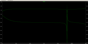
The input impedance of my topology is about 0.4 ohm , the "u" curve
the "S" curve is the phase
I see I was looking at the S curve as impedance in your plots. In my experience <10Ohm is usually low enough for most dacs hence I'm not so worried about it.
I see I was looking at the S curve as impedance in your plots. In my experience <10Ohm is usually low enough for most dacs hence I'm not so worried about it.
Input impedance VS voltage compliance determinate the
level of distortion , a level < 1 ohm is the begining of our research
to make better than AOP who is generaly used
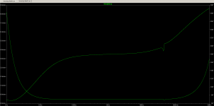
The AOP problem is the rising level of his input impedance with high frequency
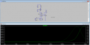
2 capture to show that point
you can see that AOP are better for low frequency
but after
Attachments
I simmed the latest version TDA1541 version and it is quite impressive. If I am reading the TDA datasheet correctly the settling time is .5 uS, which would mean the steps coming out of the DAC correspond to a 2mhz frequency, so I extended the sim to see past 1mhz and the input impedance goes lower which is great!.
I think you guys are really on to something special. The concern is holding the 0VDC input, I believe it was Ove who found that the TDA1541 needs precise 0.000DC input, he went as far as to use a simple Jfet current source to null the DC offset that is inevitable with passive I/V.
With the tube cathode are you guys seeing a stable 0VDC at the input? I imagine the Mofset helps with that? Or are we waiting for someone to build this stage? If that is the case I think I may throw my hat in and start ordering parts, unless you foresee another evolution of the design?
Hi Regal
We just try with the TDA1543 , i don't know if people build the TDA1541 version it's too new , we have just think about it
If you do it , it's important to keep in mind that is research and be carrefull
Return of information is appreciate
Perhaps is the same topology for an AD1865 , because you need +/- 1 ma
at 0Vdc too
But we can try all the version , sorry for that
The secret of this topology is that the "error correction" create by the mosfet force the voltage on cathode to tends toward 0
it' a differential correction
If this topology works in reality can you submit the result here to complete
the blog of Chanmix or tell it in Audiyofan.org
Enjoy
Last edited:
I think you guys are really on to something special. The concern is holding the 0VDC input, I believe it was Ove who found that the TDA1541 needs precise 0.000DC input, he went as far as to use a simple Jfet current source to null the DC offset that is inevitable with passive I/V.
With the tube cathode are you guys seeing a stable 0VDC at the input? I imagine the Mofset helps with that? Or are we waiting for someone to build this stage? If that is the case I think I may throw my hat in and start ordering parts, unless you foresee another evolution of the design?
Hi Regal,
As far as I understand, the TDA1541 needs 0.000V between its analog ground and its output pins. Here are quick things I would think of :
1° You set the analog ground to the converter's ground and create a -3V power supply to connect the cathod to.
2° You set the TDA's analog ground to +3V
What do you think ?
greg
Input impedance VS voltage compliance determinate the
level of distortion , a level < 1 ohm is the begining of our research
to make better than AOP who is generaly used
The AOP problem is the rising level of his input impedance with high frequency
2 capture to show that point
you can see that AOP are better for low frequency
but after
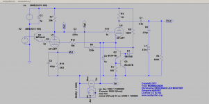
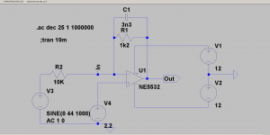
For the TDA wich is my primary concern a lot more than 10Ohm can be acceptable. But for the discussion i did this see attached schematic.
THD is 0.000333% Its still open loop and the input impedance is <100mOhm from 1Hz to 400Khz its not thoroughly optimized but I did change the operating points somewhat.
Note: C1 is a RC link to limit hf peeking as the transconductance in the sziklai pair drops of with frequency making the input impedance look inductive. But it should be possible to keep the impedance below 1ohm up over several Mhz without to much effort.
Attachments
Last edited:
- Status
- This old topic is closed. If you want to reopen this topic, contact a moderator using the "Report Post" button.
- Home
- Source & Line
- Digital Line Level
- Super common gate valve I/V converter for TDA1543