There are a few different options for the K-filter.
We could use no bias resistor, and use the k-multiplier only as a filter, and add lytic+film decoupling as usual. This is analogous to using the K-multiplier in place of a simple C-multiplier as OS has done on his previous amps.
We could also use 2SC4793/A1830 outputs, and draw an extra 100mA, for very low output impedance, and hang a 1u film off the output. This has the potential to work as well or better than lytic/film decoupling, but the idle dissipation cost is high. Could be an option. MJE180/170 outputs would allow higher bias for output impedance likely exceeding most lytics.
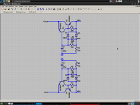
For the first option, here is the schematic I suggest. On the positive rail, the slave transistor takes 10mA of the final current, so it won't switch off in case the VAS current goes to 0. On the negative rail, since there is little danger of AC currents here, the master takes most of the bias current, which will give a lower output impedance.
LEDs are chosen for higher on voltage, so hopefully no diodes are in conduction during normal supply ripple. On music peaks which threaten to saturate the filter, the diodes should conduct momentarily to keep the filter in a normal operating range. Perhaps the filter should be tested on a real model of the amplifier, to find the best combination of time constants as a compromise between filtering and diode conduction on music peaks.
- keantoken
We could use no bias resistor, and use the k-multiplier only as a filter, and add lytic+film decoupling as usual. This is analogous to using the K-multiplier in place of a simple C-multiplier as OS has done on his previous amps.
We could also use 2SC4793/A1830 outputs, and draw an extra 100mA, for very low output impedance, and hang a 1u film off the output. This has the potential to work as well or better than lytic/film decoupling, but the idle dissipation cost is high. Could be an option. MJE180/170 outputs would allow higher bias for output impedance likely exceeding most lytics.
For the first option, here is the schematic I suggest. On the positive rail, the slave transistor takes 10mA of the final current, so it won't switch off in case the VAS current goes to 0. On the negative rail, since there is little danger of AC currents here, the master takes most of the bias current, which will give a lower output impedance.
LEDs are chosen for higher on voltage, so hopefully no diodes are in conduction during normal supply ripple. On music peaks which threaten to saturate the filter, the diodes should conduct momentarily to keep the filter in a normal operating range. Perhaps the filter should be tested on a real model of the amplifier, to find the best combination of time constants as a compromise between filtering and diode conduction on music peaks.
- keantoken
Attachments
I looked at the design package (post #188) and have to commend ostripper for his hard labour! It's a ton of work to do up schematic, simulation, BoM, PCB and construction notes for the community  I believe he's offline (moving) right now?
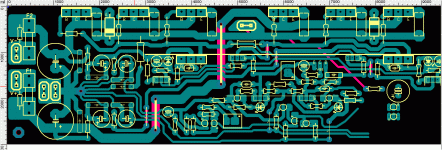
Possibly a few minor corrections; on the PCB (Rev 2.1) some designators are swapped but do not affect operation:
Q19, Q20, Q15/C18, Q21 - Q13 - Q18, Q14/C19, Q17, Q16 (pcb along heatsink edge)
Q21, Q20, Q15/C19, Q19 - Q13 - Q16, Q14/C18, Q17, Q18 (should read)
Other notes:
-D1 and D2 are 0.1A 1N914's but Bom specs 1A (1N4001?)
-D8 and D9 would be nice to show these (optionals) on schematic
-I'm not sure why Q11 is not the same type as Q8. It would also make heatsink mounting of Q11/Q12 less hassle.
Is DIY Audio doing a batch of OS or Alex_mm's pcb layout? I wasn't sure where we are right now with the project.
I believe he's offline (moving) right now?Possibly a few minor corrections; on the PCB (Rev 2.1) some designators are swapped but do not affect operation:
Q19, Q20, Q15/C18, Q21 - Q13 - Q18, Q14/C19, Q17, Q16 (pcb along heatsink edge)
Q21, Q20, Q15/C19, Q19 - Q13 - Q16, Q14/C18, Q17, Q18 (should read)
Other notes:
-D1 and D2 are 0.1A 1N914's but Bom specs 1A (1N4001?)
-D8 and D9 would be nice to show these (optionals) on schematic
-I'm not sure why Q11 is not the same type as Q8. It would also make heatsink mounting of Q11/Q12 less hassle.
Is DIY Audio doing a batch of OS or Alex_mm's pcb layout? I wasn't sure where we are right now with the project.
Precise Prereg + K-Multip + Shunt ?
Ken,
Very nice implementation, If a precise matched OP Voltages would be needed, then each rail would need the complete chain consisting: the Precision adj. pre-regulator, following with K-multiplier and the low R shunt at the OP ?
Any suggestion for the previously mentioned voltages and target currents ?
Regards
A.
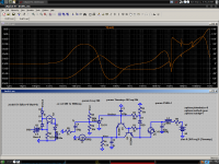
I haven't tried it, but I could put a TL431 at the output to adjust the output voltage slowly. However one reason the Kmultiplier works like it does is that the output voltage at DC depends on the input voltage; thus the voltage drop across the transistors will mostly be constant, for guaranteed low dissipation. When you add a regulator you must worry about the transistor dissipation and be careful not to exceed input voltage.
Something like the attached could work. The network C4 and R9 is necessary to reduce TL431 gain at HF so it doesn't clip into the 470uF filter cap (R9 is needed to damped a bass resonance). Simulated input filtering is plotted. This is with Cordell's models and a TL431 model I created to be very accurate to the datasheet. Output voltage is held at 50V, though I realize I'm exceeding the TL431's voltage specs (maybe a simple series R is good enough?).
Tomorrow I may make another simulation with the C4793 output and shunt bias resistor.
- keantoken
Attachments
I looked at the design package (post #188) and have to commend ostripper for his hard labour! It's a ton of work to do up schematic, simulation, BoM, PCB and construction notes for the community
Possibly a few minor corrections; on the PCB (Rev 2.1) some designators are swapped but do not affect operation:
Q19, Q20, Q15/C18, Q21 - Q13 - Q18, Q14/C19, Q17, Q16 (pcb along heatsink edge)
Q21, Q20, Q15/C19, Q19 - Q13 - Q16, Q14/C18, Q17, Q18 (should read)
Other notes:
-D1 and D2 are 0.1A 1N914's but Bom specs 1A (1N4001?)
-D8 and D9 would be nice to show these (optionals) on schematic
-I'm not sure why Q11 is not the same type as Q8. It would also make heatsink mounting of Q11/Q12 less hassle.
Is DIY Audio doing a batch of OS or Alex_mm's pcb layout? I wasn't sure where we are right now with the project.
2 power failures.... I will look at these discrepancies and report back on 9/19 (no internet currently).
The PCB should be good to etch as these are just labeling errors .
My move was both painful and difficult ... slumlords , broken houses and other assorted B_S X 2.
OS
Last edited:
Cleaned up the BOM a little to make it easier to order the parts
Is it just me or are a lot of the semiconductors not available from Digikey?
Also:
C2 - 270pF film /w 7.5mm LS is not a common size. Is this correct? 5mm can be had easily.
C13, C17 - can be either 470 uF or 1000 uF? What difference will it make? Are there any height restrictions, or is the height of this cap what will determine overall thickness of the package?
C21 - is the same as C4,C10,C12,C14,C16 but needs to be 250V. C4,C10,C12,C14,C16 can be found in 250V but need to be X7R (I assume ceramic). Is this OK? End result will be C4,C10,C12,C14,C16,C21 in 0.1uF 250V X7R ceramic cap
Attachments
Last edited:
Or, instead of X7R, MKP is a possibility. Is the capacitor order of preference aluminum -> ceramic -> film -> mica, if not otherwise noted?Cleaned up the BOM a little to make it easier to order the parts
Is it just me or are a lot of the semiconductors not available from Digikey?
Also:
C2 - 270pF film /w 7.5mm LS is not a common size. Is this correct? 5mm can be had easily.
C13, C17 - can be either 470 uF or 1000 uF? What difference will it make? Are there any height restrictions, or is the height of this cap what will determine overall thickness of the package?
C21 - is the same as C4,C10,C12,C14,C16 but needs to be 250V. C4,C10,C12,C14,C16 can be found in 250V but need to be X7R (I assume ceramic). Is this OK? End result will be C4,C10,C12,C14,C16,C21 in 0.1uF 250V X7R ceramic cap
I hate this 30 minute edit limit.
C5 - does not use a common size. Only available one on Digikey that matches is this one, which doesn't seem ideal. However, if you remove your D=6.0 mm restriction, then the 8.0 mm caps work very well (I checked PCB and it seems like more than 6 mm is available).
Last edited:
To recap:
C13 - misprint/poor typography on PCB (hard to read)
C13,C17 - what's the difference between 470 uF and 1000 uF? Any height restrictions or the height selected per user preference?
C18,C19 - can these be NP0 instead of mica?
C2 - is lead length crucial to minimize inductance? If not, film, ceramic, or mica can be used? Candidate 1 , candidate 2
C4,C10,C12,C14,C16,C21 - can be X7R or need to be film?
C5 - should not be D=6.0mm
Q... - bunch of devices not available from Digi-Key
I've cleaned up the BOM a little more... see attachment. Use at your own risk until reviewed by management.
Attachments
Last edited:
This project is not on hiatus, I hope?
i believe it is until ostripper finishes his move and regains internet access , gets the gerbers to variac and variac gets them produced and in the store .
This project is not on hiatus, I hope?
No , it is not. I read the mention of the small labeling issues and am reviewing them.
I rented for $1700... house was near collapse. Had to move a SECOND time , My present house had reverse polarity outlets (corrected). Local ISP took 18 days to connect me online.
In short ... After much hassle , I am back
.C13 - misprint/poor typography on PCB (hard to read)
C13,C17 - what's the difference between 470 uF and 1000 uF? Any height restrictions or the height selected per user preference?
C18,C19 - can these be NP0 instead of mica?
C2 - is lead length crucial to minimize inductance? If not, film, ceramic, or mica can be used? Candidate 1 , candidate 2
C4,C10,C12,C14,C16,C21 - can be X7R or need to be film?
C5 - should not be D=6.0mm
C13 is easily readable (image 1), especially if screened by a good manufacturer.
C13,17 are either 7.5mm or 10mm lead space. As the main decoupling , they should be as large as possible. All 16/25mm's will fit , any height as can be accommodated.
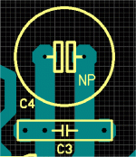
C18,C19 are capacitive stoppers for the drivers. Depending on driver- Cob/Ft and the layout, they can be 47-150p... AND NP0 IS acceptable (nikko, adcom use these).
(image 2 below) is the standard 7.5/10mm poly cap pad ... I found DOZENS of acceptable sourcing's from wima and other manufacturers for most of these .1uf (100-250v) units. Film is the most reliable for HF bypass with very low ESR in these conditions. C4 is the DC blocking NP cap (220uF 25-50V).
C5,9 's lead spacing is correct (3.5mm). My 10uf and 22uf panasonic electro's are just 5mm in diameter. They fit my present amp perfect ... I used the same pads. ALL these pads have been stuffed on my home amps and are exact to the real parts. On a new part , I will even print out the pad and inspect for fit and the aesthetics of the screenprint.
Yes , C2 can be made more universal (5 , 7.5mm)
I have not squandered my offline time , as I will review this one yet again and
have done 2 more amps (luxman triple -below 3) and a lateral luxman (secret project
).OS
Attachments
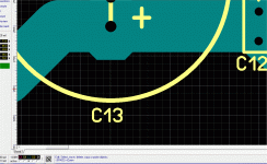
Both your BOM and the PCB show 5.0 and 7.5, looks like.C13,17 are either 7.5mm or 10mm lead space. As the main decoupling , they should be as large as possible. All 16/25mm's will fit , any height as can be accommodated.
I take it to mean that C3,C10,C12,C14,C16,C21 should all be film?(image 2 below) is the standard 7.5/10mm poly cap pad ... I found DOZENS of acceptable sourcing's from wima and other manufacturers for most of these .1uf (100-250v) units. Film is the most reliable for HF bypass with very low ESR in these conditions.
Your BOM says:C4 is the DC blocking NP cap (220uF 25-50V).
C3 -- -- capacitor, 220µF NON-POLAR 12.5mm D 5MM LS
C4 -- -- capacitor, 100nF (.1uF) 7.5 OR 10MM LS
I assume that you swapped these by mistake - I will correct on my version.
All I see on Digikey for 22 uF lytics, 3.5 mm LS, are 8.0mm diameter caps.C5,9 's lead spacing is correct (3.5mm). My 10uf and 22uf panasonic electro's are just 5mm in diameter. They fit my present amp perfect ... I used the same pads. ALL these pads have been stuffed on my home amps and are exact to the real parts. On a new part , I will even print out the pad and inspect for fit and the aesthetics of the screenprint.
Let me know what changes you will be making to the PCB - your original one looks like it has 7.5/10 mm spacing for C2.Yes , C2 can be made more universal (5 , 7.5mm)
Any idea what to do about the hard-to-find transistors?
Sorry to hear about all the housing hassles.
Attachments
Last edited:
Let me know what changes you will be making to the PCB - your original one looks like it has 7.5/10 mm spacing for C2.
Better yet , anything I do will be view-able/downloadable here :
HFS /D:/WEBSITE/DIYA-amp/
This link is "home" for the project.

PS . State the "hard to get" semi's , I will research alternatives.
OS
Last edited:
Q1,Q2 -- MPSA18/SS9014 -- MPSA18RLRAG is available at Digikey
Q10 -- 2SA1381 -- not available at Digikey, Mouser; Newark recommends MJE350G
Q11,Q12,Q13 -- 2SC3503 -- not available at Digikey; 2SC3503FSTU available at Mouser (scheduled to become obsolete)
Q14 -- MJE15032 -- MJE15032G is available at Digikey
Q15 -- MJE15033 -- MJE15033G is available at Digikey
Q16,Q17,Q18 -- MJL3281 -- MJL3281AG available at Digikey
Q19,Q20,Q21 -- MJL1302 -- MJL1302AG available at Digikey (low quantities) and Mouser
Q3,Q4,Q7,Q8 -- KSC1845 -- KSC1845 (various types) available at Mouser
Q5,Q6,Q9 -- KSA992 -- KSA992 (various types) available at Mouser
------------
2SA1381 is the only difficult one; also, 2SC3503 is available, but not in huge quantities.
So to recap yet again:
C2/C3 - please add one more hole to allow for 5.0 mm LS.
C5/C9 - I suggest that an 8.0 mm diameter cap will work, after checking with a vernier on a scale printout.
C13/C17 - please add an extra pair of holes to allow for 10.0 mm LS.
Also,
C20 - please add 2 more holes to allow for 15.0 mm, 20.0 mm LS (required for polypro caps)... unless polypro caps offer no advantages vs polyester caps in this application.
C12/C16 - if you can move C11/C15 to the right a little bit, please do; a 5mm thick cap will be a tight squeeze here.
C10/C14/C21 - can you add a little more space between these caps? 5mm thickness caps will not fit here... you might have to move R32 and C11 to allow that, though.
Last edited:

- Home
- Amplifiers
- Solid State
- diyAB Amp - The "Honey Badger"