ClothEar
Realy interesting question
There is quite a bit I also do not know and get blown away by post such as Papa mention of P3 and post 10855 SCH show quite a few values changes
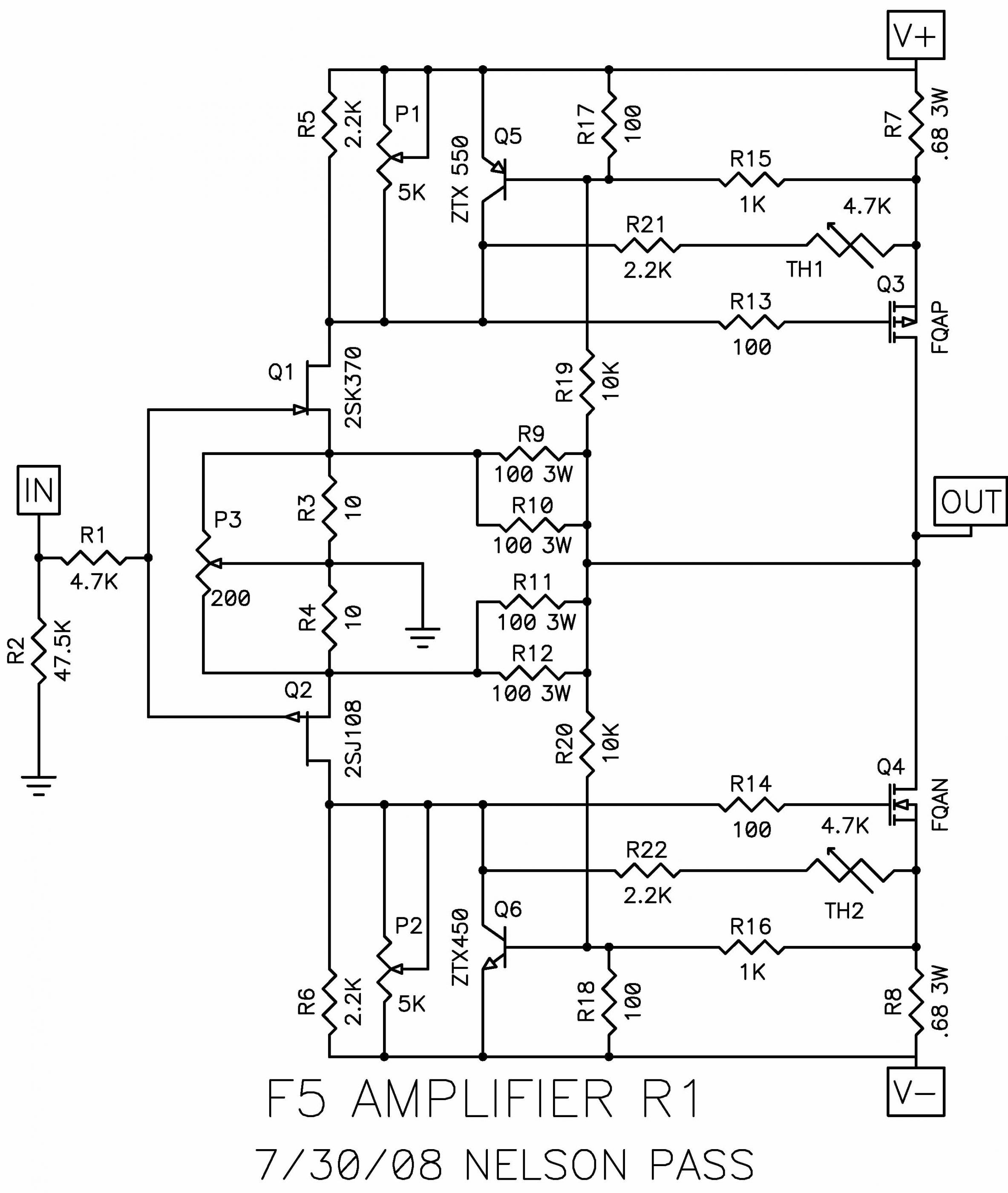
Such as 0.68 source resistors and 10 to 1 relationship on the Imput resistors R13/R14 are100 homs in that one and few conection are different as well as the thermistors are after R7/R8
Papa said that almost any change would efect the way the F5 sound.
I have tried P3 and left it out after blowing a couple of mosfets as Bias got realy hi even with a 10 turn pot and very small turn on it.
I have to finish off a second channell with Cascode and 2 paralel J fets as mentioned in another post before I can post my listening impressions on that change.
So far I can say that the first channel on which I made the change sems to have less distorsion and lover gain but this is based purely in what I can ear as my knolledge of electronics is wery limited.
As I am etching my own boards is quite easy for me to put a few extra pads in and try things out.
But like you I would realy apreciate if we could get same pointers on the caracter of those "small" changes
Realy interesting question
There is quite a bit I also do not know and get blown away by post such as Papa mention of P3 and post 10855 SCH show quite a few values changes
Such as 0.68 source resistors and 10 to 1 relationship on the Imput resistors R13/R14 are100 homs in that one and few conection are different as well as the thermistors are after R7/R8
Papa said that almost any change would efect the way the F5 sound.
I have tried P3 and left it out after blowing a couple of mosfets as Bias got realy hi even with a 10 turn pot and very small turn on it.
I have to finish off a second channell with Cascode and 2 paralel J fets as mentioned in another post before I can post my listening impressions on that change.
So far I can say that the first channel on which I made the change sems to have less distorsion and lover gain but this is based purely in what I can ear as my knolledge of electronics is wery limited.
As I am etching my own boards is quite easy for me to put a few extra pads in and try things out.
But like you I would realy apreciate if we could get same pointers on the caracter of those "small" changes
Hi Huseyin,
One thing I would do is find some discrete diodes (fast, soft recovery types) and discard those KBP block bridges that do add a definite "edge" to the sound that's nearly impossible to get rid of.
I assume there are 4 Kendeils 47,000uF caps? What are the black 470uF/200 Daewoo caps for?
If you're going to mount the power fets to the top flat bar that's holding the 2 seperate heatsinks together, there is quite a bit of added thermal resistance between the plate and the heatsink - suggest using a smaller bar, or angle bracket, to hold the top and bottom edges of the heatsinks together and fasten o/p fets to heatsinks directly - more efficient and simpler.
Also, the angle bracket can be used to mount the bottom and top covers.
... just my 2 cents.
Are Q3 & Q4 still being biased at 1.3 amps in this revised F5 circuit (F5 Amplifier R1; 7/30/2008)? Am asking as that answers the question as to what voltage drops to look for across R7 & R8 when adjusting P1 & P2. (1.3 A * 0.68 Ohms = 0.88 V)Hasn't this been around?

Thanks
ClothEar you welcome.
dnewman
About R7 R8 I have tried 0.22 Homs Futabas MPC 74 with Paralell Toshibas as I was biasing each at over 2 A and the 0.47 Where a bit hot, sound wise all was fine (IMO I like farchild sound better).
I am not going in the math for it as there are much better "professors" around here but I would wach out for the power rating of those.
Last edited:
Hi Huseyin,
One thing I would do is find some discrete diodes (fast, soft recovery types) and discard those KBP block bridges that do add a definite "edge" to the sound that's nearly impossible to get rid of.
I assume there are 4 Kendeils 47,000uF caps? What are the black 470uF/200 Daewoo caps for?
If you're going to mount the power fets to the top flat bar that's holding the 2 seperate heatsinks together, there is quite a bit of added thermal resistance between the plate and the heatsink - suggest using a smaller bar, or angle bracket, to hold the top and bottom edges of the heatsinks together and fasten o/p fets to heatsinks directly - more efficient and simpler.
Also, the angle bracket can be used to mount the bottom and top covers.
... just my 2 cents.
Thanx jameshillj.
I think the fast diodes will be better.
I just have 2 kendeils,but ı can add the 10,000uf caps,I put the black caps instead of 4700uf 25v by mistake.
yes I'll mount the outp. fets as you first said.
I'll keep in touch the forum on my project.
Hasn't this been around?
Hi,
I'm a long time lurker who's just finished reading this thread
 and I'm putting the finishing touches on my first F5 build. I have a little confusion to clear up before I put the "firstwatt" to my build.
 My build is on Peter Daniel's version of the PCBs and I bought the bits and pieces from TechDIY as "F5 kits". The Peter Daniel's board follows the original schematic, but the TechDIY kit is for the "R1" version. It was no problem to put a couple jumpers to modify the Peter Daniels board to follow the "R1" schematic and then install my "R1" parts kits.
Two questions before I risk some smoke.
What is the function of R1 (4.7k) on the new (left side) schematic ? The input resistor divider R9-R10 of the original (right side) schematic has changed in the new drawing. Should I jumper my board to match the new "R1" schematic for the connections of R1 (4.7k signal input resistor) ? I'm not understanding what current flows through R1 as drawn and what it's function is ?
I'm guessing the only difference in the initial set up of the original and "R1" version is to center (measure) the P3 pot prior to power on ? Any other caveats ? Is P3 useful for anything other than changing the harmonic distortion distribution ?
Thanks for any advice, and thanks especially to NP for the design and all the regulars for this entertaining thread, even though it is a bit long. It has been kind of like a long novel with a surprise twist to the ending. The new "R1" version schematic cleared up all kinds of "WTF"
on my part, as I compared my boards to my parts kits and read the first thousand pages or so.R1 and R2 in the Rev 1 F5 schematic fulfill the same roles as R9 and R10 in the original F5 schematic. Just different values. As described in the F5 Operation and Service Manual, R9 [now R1] is to prevent parasitic oscillation of the input JFETs, and R10 [now R2] is to provide a reference to ground for the input JFETs when nothing is attached to the input (i.e., the input is "floating"). See the section entitled "Actual Working Circuit" of the manual for these descriptions. In the Rev 1 F5 schematic, the input JFETs see ground through R1+R2 as opposed to seeing it through just R9 of the original schematic. 100k vs. 52.2k? Either works. However, I am curious as to the change from 1k to 4.7k for the "input" resistor. (I've not studied the circuit carefully enough to see what drove that change.)Two questions before I risk some smoke.
What is the function of R1 (4.7k) on the new (left side) schematic ? The input resistor divider R9-R10 of the original (right side) schematic has changed in the new drawing. Should I jumper my board to match the new "R1" schematic for the connections of R1 (4.7k signal input resistor) ? I'm not understanding what current flows through R1 as drawn and what it's function is ?
I'm guessing the only difference in the initial set up of the original and "R1" version is to center (measure) the P3 pot prior to power on ? Any other caveats ? Is P3 useful for anything other than changing the harmonic distortion distribution ?
I believe that you can simply omit P3. Note that in some earlier posts, there has been mention of slight adjustments to P3 burning out transistors....
Since the values of the source resistors for Q3 and Q4 have been changed from 0.47 to 0.68 Ohms, the target voltage across the source resistors has changed as well. The source resistors are R11 and R12 in the original schematic (0.47 Ohms * 1.3 A = 0.6 V) and they are R7 and R8 in the Rev 1 schematic (0.68 Ohms * 1.3 A = 0.88 V). I'm here using a bias current of 1.3 A.
Attachments

Thanks for the response. It definitely answers enough of my questions to let me have a first try at bringing my amp up. I will remove P3 from my boards for the intitial set up and listening. Other than that, I am using the "R1" schematic and component values. Next weekend is when I have time set aside to run through the initial start up. Hopefully it will be music rather than smoke.
P3 in R1 schematic have same purpose as additional source resistor( of output mosfet) on one side - which you can see on any original FW F5 picture .
fine fiddle with signal gene + THD meter is needed for setting .
what's important is knowing that you must be careful , approaching extremes of that pot
fine fiddle with signal gene + THD meter is needed for setting .
what's important is knowing that you must be careful , approaching extremes of that pot
non-matching transconductance
I am making an F5 (with multiple output devices) in little steps.
1) test the mosfets, for 0,6 amp conducting. I have 2SK175/2SJ55.
- Based on that I compiled a list for the matching of units for the two channels.
2) test the jFETS, and group them (match is a big word)
3) measure the feedback resistors and match them within 0,01 dB.
4) populate the board with fb-resistors and the trimpot 5K, the jFETS (with a 2SK170 of Ids of 11 mA; 2SJ74 of Ids of 12,5 mA).
5) dial in the bias voltage I want (for the 600 mA per device, about 1,5 volt for this test step). The N-side was 235 ohms, the P-side 196 ohms
6) Now the awkward step: apply a test-signal to the input and measure the voltage on the two drains. [I have not connected the outputs yet.]
- There is a difference of 10 dB between the two halves , and just for certainty I connected a 2SJ74 of 20 mA - and that gave a difference of almost 13 dB.
This would imply that there is a difference in closed-loop feedback amount between the topside of the amplifier and the bottom side. (amplification of both halves is the same of course).
Is this normal?
Would it be OK to just go ahead and close the loop?
Or should I test the amplification of all jFETS on a standard resistor (1k) first? I am afraid there is always a difference between the DC selection and such a transconductance selection. So it is a never ending selection.
albert
Hi triode
What is the difference in VGS between positive and negative channels Mosfets?
I have FQP19N20 and FQA12P20 and positive channels mesure much hier at same rail voltagge current and themperature.
I am interested in this. I was measuring the P-channel on my remaining P-channel FQA, and it was measureing -5v vgs. I was not thinking this is right.
The N channels were running ~ 3.5-3.7 with a 25v power supply.
Hi Bksabath,
the power units are, one channel:
2SJ55 average 1,65 volt Vgs for 0,6A current.
#7 100 mA 0,714; 600mA: 1,656 -
#14 100 mA: 0,716; 600mA: 1,647
#9 100 mA: 0,718; 600mA: 1,638
2SK1751,39 volt Vgs for 0,6A current.
#8 100 mA: 0,609; 600mA: 1,401- average
#22 100 mA: 0,609; 600mA: 1,391
#21 100 mA: 0,611; 600mA: 1,380
(I can make 4 closely matched sets out of 22 devices, not bad)
So I turned the potmeters to get this voltage between drain of jFET and the power rail; would later need to cater for the source resistance too, is 0,45 ohm, so 0,25 v extra.
The Toshiba's have a quite good tolerance, compared to the Fairchilds. Maybe it works in my disadvantage, Michael.
This is a big difference from the voltages of Tea-Bag.
My JFETS :
2SK170 BL
# 0 ohm 5 ohm 10 ohm 15 ohm 20 ohm
#12 7,03 6,05 5,38 4,82 4,39
#6 7,04 6,08 5,41 4,86 4,43
#4 7,08 6,11 5,47 4,86 4,42
#8 7,45 6,4 5,67 5,08 4,63
#11 7,47 6,43 5,71 5,12 4,66
#1 7,58 6,49 5,75 5,15 4,68
#13 7,58 6,52 5,79 5,19 4,73
#16 7,86 6,74 5,97 5,34 4,86
#3 8,11 6,92 6,11 5,45 4,95
#5 8,15 6,95 6,14 5,49 4,99
#7 8,49 7,26 6,42 5,73 5,21
#2 9,07 7,72 6,8 6,06 5,49
#14 9,32 7,92 6,97 6,21 5,63
#9 9,53 8,08 7,11 6,33 5,72
#10 9,65 8,19 7,2 6,41 5,80
#15 11,02 9,28 8,13 7,21 6,52
2SJ74 BL
# 0 ohm 5 ohm 10 ohm 15 ohm 20 ohm
#I 19,1 17,86 16,86 15,98 15,20
#II 20,32 19,13 17,97 16,98 16,15
#III 12,5 11,62 10,98 10,42 10,05
So if I take the #1 J74 with the #12 K170 I have the same transconductance, but not the same Ids.
ps. I use a 1 kHz test signal on the regular input of the boards.
albert
Add in 51r to the top and bottom legs of P3 before tapping into the Source connections.
This raises the total resistance (of the bypass route) to ~300r and gives an adequate adjustment range for the 10r R3 & R4.
Gain of the first stage is P1/[(1/gm)+Rs] and is nominally 10, so adding 50R is going to get a bit closer to 10X from the original. You don't have to add P3 -- you can parallel values against one or the other against R1/R2 (Refdes from the original schematic).
I experimented with this and it doesn't take much tweeking of P3 to lower the THD. I'll state again, however, that right out of the box the F5 THD% is 0.006% to 0.008% @1W into 8R
As there's still a bit of water in the workshop, I won't be able to demonstrate with a chart for a while!
- Home
- Amplifiers
- Pass Labs
- F5 power amplifier