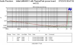
We all knew that layout pays vital role in amp performance. Here is an evidence. The amp under test is LME49811 with two-pair NJL3281D/1302D.
From left: 1kHz for previous version power board, 1 kHz for new version power board, 10 kHz for previous version power board, 10 kHz for new version power board
The performance for 8 Ohm is nearly the same for both boards. However, it is very clear that the new board achieves better performance (lower THD and higher clipping level) for heavier loads.
I just told you that I did not make a very good boardor I am improving.
I am going to take trace resistance measurement. See whether I can get some useful data.
Panson,
You may be right, but, I also thought that your new boards had significantly more on board capacitance. I remember reading a thread where Bob Cordell was talking about the benefits of on board capacitance. He was describing the "violent" voltage/current swings at the output transistors under heavy load as they switch on and off in the class B mode and how this switching caused extreme things to happen at the power supply to these devices. The on board capacitance, close to the pins of the (significantly closer than the main supply caps) would absorb or dampen these extremes, reducing their influence on their counter parts as well as the driver transistors.
Maybe you should put the same amount of capacitance on the early version boards and then compare. At a minimum it would eliminate one variable.
Regards,
Ken
Maybe you should put the same amount of capacitance on the early version boards and then compare. At a minimum it would eliminate one variable.
Ken,
Yes, I added the same amount of onboard cap on the old board for comparison.
Panson
Ken,
Yes, I added the same amount of onboard cap on the old board for comparison.
Panson
Ok, so much for that theory
What do you think you have done to improve the new boards?
Ken
Hi,
is the result timed 10:25:31 of the old PCB?
Can you give us a link to pics of both PCBs for comparison?
That particular plot is for the new board.
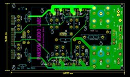
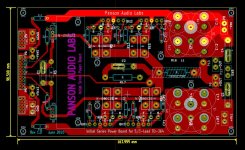
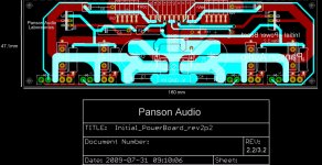
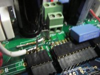
Here are the layout of old and new boards.
I tested both boards without output coil and Zobel RC.
Attachments
What do you think you have done to improve the new boards?
The extra onboard caps do not make very big different.
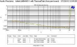
Left: no extra onboard cap
Right: with extra onboard cap. better performance in 4 Ohm, very slightly improvement in 2.7 Ohm (assuming this is not measurement error).
I am doing tests for why the new board is better. The new one got more space for better/easier routing. I think this is the key factor. The net resistance of some critical traces of the new board does not lower than the old one. As can be seen from the plots, the new board got lower THD. It should be contributed by component placement and routing pattern instead of thicker traces.
Attachments
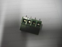
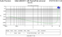
I just found the root cause of the problem. This is not layout at all.
This is the connector used in the old board!!! Take a look of the plot to see what it does!
This is the connector used in the old board!!! Take a look of the plot to see what it does!
Attachments
Last edited:
I just found the root cause of the problem. This is not layout at all.
I might be wrong for saying not layout related. The 2.7 Ohm curve of the old board with connector issue fixed is flat from 10 V whereas that of the new board does not. It may indicate there is something going on not found yet. My test is thus continued.
It may indicate there is something going on not found yet. My test is thus continued.
Its really great work you're doing here Panson!
I think you've got a slight grounding problem - slight, but this amp has very low distortion so I think its making a difference.
Your onboard decoupling caps share some common impedance with the output ground and the ground power input. I suggest isolating the individual current paths rather than doing a ground fill.
I take it that P10 is the ground to the load and P11 is the ground power input, right? Look to see that the gap between these lugs has current flowing to the decoupling caps too. For best performance the current to the decouplers must have its own path, not in common with any other. Current flowing into those caps tends to be very distorted and surprisingly large. Even a short very wide track to them can introduce a big enough voltage drop to downgrade the measured distortion.
Hi Abraxalito,
Thanks for your input.
I don't use the onboard output- (output ground) in all the tests. The output ground is from the 0V of power supply board.There are four connections to the supply 0V: two for LME49811 driver board ground (one for decoupling caps and one for NFB, input), one for power board ground ( essentially the ground path for decoupling caps) and one for output ground.
Panson
I just found the root cause of the problem. This is not layout at all.
This is the connector used in the old board!!! Take a look of the plot to see what it does!
I'm not sure I understand what happened, did the connector melt? Or what?
Ken
Mark and I did not specifically discuss those caps. What is your experience?
I usually use 100nF in these positions, and didn't pay that much heed to the schematic until a bit later. When I played around with 470n and 680n the sound seemed more "developed". There wasn't any measurable difference in performance, just a subtle change in the way it sounded. I do have some of these caps mounted to the bottom of the board as it's the only way I could get them close to the chip and still maintain the consistent layout. I've variously used WIMA PP, BC Components polyester and 100n ceramics.
I don't have my notebook with me at the moment, will have to see if there was anything else to note.
I'm not sure I understand what happened, did the connector melt? Or what?
Ken
No. They are just not linear at high current.
I eventually found the root cause for the old board inferior performance compared to the new board. In the new version power board, there two 10R resistors for each rail. These 10R together with the decoupling caps on the LME driver form LPFs to make a cleaner supply voltage for the LME chip. The old board does not have the resistors. After I added the 10R resistors, the performance with the old power board is identical to that of new new power board.
Based on the result, separate power supply for the LME board may lead to better performance. Will give it a try.
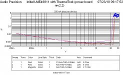
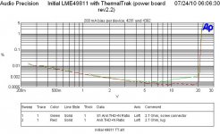
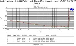
1 kHz THD vs level plots
Left: without the 10R resistors
Right: with the 10R resistors
Based on the result, separate power supply for the LME board may lead to better performance. Will give it a try.
1 kHz THD vs level plots
Left: without the 10R resistors
Right: with the 10R resistors
Attachments
I haven't experienced any severe noise issues with the LME drivers -- but I use a radial system of grounds as Mark recommended in his LM4702 application note. You can not use a ground plane. I've also used a small decoupling resistor on Vcc/Vee of the chip, something like 10 ohms. Mark was also pretty specific about the decoupling caps on the power pins of the device. for economy of space I mounted these on the bottom of the printed circuit boards I had burned.
I believe the reason that these driver chips are "susceptible" to noise is that they stand out there like a high gain radiator (antenna) --
You actually can use a ground-plane with excellent results. I finally bite the bullet and went for ground-plane topology, after being told many times ground-planes are no good for amplifiers
Bruno Putzeys from Hypex finally convinced me, and thought us how to do it. If you take very good care about placement of components, (start with a empty piece of paper and draw out the ground loops out). Another point, my amplifiers are all feed balanced, so the negative input reference to the output of the driver opamp instead of the ground-plane. That can be the biggest reason why I don't have any ground-loop related hum.
I used the LM4702 in a multichannel amplifier application, with one unbroken total ground-plane, and the THD measurements are below the limits of what I am able to measure (0.0005%). I never achieved this results with star grounding. Noise floor is inaudible low.
Second benefit, I can put my cellphone in front of the circuit and no "buzz" anymore over the speakers.
A ground-plane design does sound different then a star-ground design. The same circuit with ground-plane sound more analytical, and a more airy in the high-end. and it seems subjectively speaking, more resolving details. Most strange was that the bass seemed a factor 10 tighter with the ground-plane. Can't really explain why in technical terms, but it was very noticeable in a listening panel of people.
One other note though, my design is a 4 layer board, and all high current supply lines and loudspeaker lines are all stacked on top of each other and are kept away from the LM4702 and other low current stages. Magnetic influences are minimized.
My opinion is, with careful design and routing, one can make superior results with ground-plane topology, and the LM/LME driver chips can work perfectly with ground-planes.
There is a understandable "fear" fro ground-planes, but we should overwin those, learn from RF experts and papers and give it a try.
With kind regards,
Bas
There is a understandable "fear" fro ground-planes, but we should overwin those, learn from RF experts and papers and give it a try.
Hi Bas,
Thank you very much for your sharing. Why people fear from ground planes for power amp layout? Because we want to see how we control/guide current path?
Here is a good article/useful for ground plane. http://www.hottconsultants.com/pdf_files/june2001pcd_mixedsignal.pdf
Panson
Why people fear from ground planes for power amp layout? Because we want to see how we control/guide current path?
For me, when designing a DAC, certainly I will use a ground plane for the DAC itself. That's because its a digital part, it switches at very high frequencies. In this case, the ground plane gives the power supply low enough inductance so that the power supplies stay within spec at the switching instants. Normal wiring has too much inductance.
For a class B or AB amplifier, there's no high speed switching. So the ground plane isn't needed for very low inductance. It still has value for screening against RF - Bas's point about his cellphone is a really good one - I'd like to know how it is that ground planes prevent interference from cellphones. Then I might be persuaded to try them in my amplifiers.
For myself, yes I really want to control where the currents in the grounds flow. Its possible to use a ground plane only for screening and not to deliver power supply currents - this might be the best solution.
Very interesting to hear your listening impressions about ground planes Bas - in that listening test, was the circuit otherwise identical other than the ground plane? Was the ground plane being used for both signal AND power?
<edit> I'm also curious about your 'feed balanced' remark. Do you mean you're using differential signals in your circuits?
Last edited:
Panson,
Have you done any experiments using separate elevated power supply for the frontend and checked the results.
I have read most of this and other threads on these chips but no input on separate power supplies.
Also, have you given any thought to providing a pcb on your website for the power mosfets and a driver for say 3 or 4 pairs. The schematic is vague on the exact parts for the driver part of the output when using mosfets.
Tad
- Status
- This old topic is closed. If you want to reopen this topic, contact a moderator using the "Report Post" button.
- Home
- Amplifiers
- Chip Amps
- Comparing LME49810, 49830 and 49811