Hi Ian,
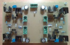
enclosed a picture of my UGS board, the schematic and FFT plots.
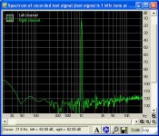
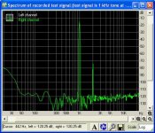
The first FFT is from the soundcard in loopback mode only. The second FFT is with soundcard and UGS board. For the measurements I used a Terratec Phase26 USB. As I mentioned yesterday, it has only single ended inputs and outputs. Therefore the second FFT plot shows only the spectrum of the positive output voltage. A more professional soundcard with balanced inputs and outputs like the E-MU 0404 would be better for my requirements. The software I've used is RMAA from Audio Rightmark. It is available for free. SpectraPLUS is more powerful and more adequate for such measurements, but it is not for free, after trial period of 30 days you have to buy the software.
Sorry for the bad quality of the board picture.
Uwe
enclosed a picture of my UGS board, the schematic and FFT plots.
The first FFT is from the soundcard in loopback mode only. The second FFT is with soundcard and UGS board. For the measurements I used a Terratec Phase26 USB. As I mentioned yesterday, it has only single ended inputs and outputs. Therefore the second FFT plot shows only the spectrum of the positive output voltage. A more professional soundcard with balanced inputs and outputs like the E-MU 0404 would be better for my requirements. The software I've used is RMAA from Audio Rightmark. It is available for free. SpectraPLUS is more powerful and more adequate for such measurements, but it is not for free, after trial period of 30 days you have to buy the software.
Sorry for the bad quality of the board picture.
Uwe
Attachments
Not sure about compensating for the loss of gain by decreasing R6 though. This will increase the current in both input and second stages but I doubt it will have a huge impact on gain. The gain is determined largely by the ratio of R12 to R7 (and the same for the other three quadrants).
Ian.
Of course you're right. Maybe it was too late yesterday evening
")
For keeping the same OLG for the second stage in case R6 is decreased the source resistors of the mosfets have to be increased as well.
It seems to be hard to find the optimum operating conditions for your requirements (high CL gain, high CL bandwith, less neg feedback, high output voltage swing). My requirements are more relaxed. Basically I need only a single to balanced converter with some gain in the range of 2 for driving my balanced F5.
Nevertheless, I think spice simulations are best suited for such optimizations. Do you have appropriate models for the mosfets you use? So far I haven't found spice models for IRF610/9610 on the net.
Regards, Uwe
Uwe,
Thanks for publishing your circuit and distortion measurements. I'll investigate both the software and sound cards you mention (I'm no expert in either).
Regarding your comments on my requirements, I'm afraid you are exactly right in it being difficult to meet all the requirements. Increasing the output device source resistors for example compromises both the output swing and decreases the overal gain. Also the diff pair current cannot be reasonably increased beyond a certain point (less than Idss) to accommodate the signal swing. That is why I suspect I will need to find some better output devices. I will check that it is these that are dominant first though although I suspect the diff pair cascoding will give a wide bandwidth in the first stage.
I do have models for IRF610, 9610 and similar (I am actually using IRF510 and SFP9510 in my circuit). I can publish these if you like but I don't have them on this computer so it will have to be later.
Ian.
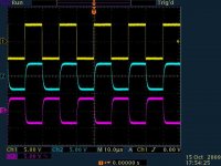
Ian,
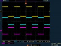
as promised, some scope plots. The input voltage (top trace) is 10Vpp, the middle and bottom traces are the output voltages. The left plot is with 10kHz, the right one with 50kHz.
I would be glad if you would post the spice models for IRF610/9610 and/or IRF510/9510 you use. Thanks a lot.
Have you checked if Toshiba offers mosfets with lower Cgd? I'm thinking about to replace the IRFs with 2SK2013/2SJ313 in my UGS.
Regards, Uwe
Attachments
Hi Uwe,
I would say the performance you are seeing with a 50KHz square wave is pretty impressive. Why do you want to change the MOSFETs? The Toshiba devices you mention are laterals and hence have lower transconductance (0.7S) than the IRFs (2S). They also have a lower Vgs so you will need to change the resistor values round a bit. Given that they don't have that much lower Cgd (17 rather than 20pf) I am not sure it would be worth the change.
I have a few suggestions to make regarding your circuit which I will try and write up shortly and post. Maybe you will like them but even if not, hopefully food for thought or experimentation.
I'll post the spice models this weekend when I have access to my home computer.
Ian.
Hi Ian,
I agree with you that the mentioned Toshibas don't have the better spec then the IRFs. I'm just curious because I use 2SK1530/2SJ201 in my F5 and I'm very happy with the resulting bias stability and sound, both is a bit better then with IRFP240/9240. The latter is of course very subjective. So maybe one day I give them a try. But they are expensive and it's hard to find them.
Please feel free to post any suggestions about the circuit, I appreciate any new ideas and thougths. That's the reason why we are here, isn't it?
Regards, Uwe
BTW, Fairchild seems to have promising mosfets too, like the FQP5N50C and FQP3P20.
Hi Uwe,
Spice models as promised:
.model IRF610 NMOS(Level=3 Gamma=0 Delta=0 Eta=0 Theta=0 Kappa=0.2 Vmax=0 Xj=0
+ Tox=100n Uo=600 Phi=.6 Rs=.5804 Kp=20.77u W=.45 L=2u Vto=3.886
+ Rd=.5781 Rds=888.9K Cbd=220.5p Pb=.8 Mj=.5 Fc=.5 Cgso=517.7p
+ Cgdo=61.68p Rg=.2597 Is=1.647p N=1 Tt=295n)
*$
.model IRF620 NMOS(Level=3 Gamma=0 Delta=0 Eta=0 Theta=0 Kappa=0.2 Vmax=0 Xj=0
+ Tox=100n Uo=600 Phi=.6 Rs=.114 Kp=20.39u W=.23 L=2u Vto=3.083
+ Rd=.3209 Rds=888.9K Cbd=650.2p Pb=.8 Mj=.5 Fc=.5 Cgso=3.996n
+ Cgdo=168.7p Rg=7.473 Is=59.21p N=1 Tt=610n)
*$
.model IRF9610 PMOS(Level=3 Gamma=0 Delta=0 Eta=0 Theta=0 Kappa=0.2 Vmax=0 Xj=0
+ Tox=100n Uo=300 Phi=.6 Rs=.721 Kp=10.37u W=.64 L=2u Vto=-3.814
+ Rd=1.524 Rds=888.9K Cbd=222.3p Pb=.8 Mj=.5 Fc=.5 Cgso=1.517n
+ Cgdo=30.29p Rg=2.4 Is=886.1E-18 N=4 Tt=1100n)
*$
.model IRF9620 PMOS(Level=3 Gamma=0 Delta=0 Eta=0 Theta=0 Kappa=0.2 Vmax=0 Xj=0
+ Tox=100n Uo=300 Phi=.6 Rs=.339 Kp=10.15u W=1.4 L=2u Vto=-3.735
+ Rd=.6365 Rds=888.9K Cbd=426.4p Pb=.8 Mj=.5 Fc=.5 Cgso=1.359n
+ Cgdo=32.22p Rg=1.106 Is=48.34E-18 N=3 Tt=670n)
*$
.model IRF510 NMOS(Level=3 Gamma=0 Delta=0 Eta=0 Theta=0 Kappa=0.2 Vmax=0 Xj=0
+ Tox=100n Uo=600 Phi=.6 Rs=.4508 Kp=20.68u W=.64 L=2u Vto=3.697
+ Rd=21.08m Rds=444.4K Cbd=366.5p Pb=.8 Mj=.5 Fc=.5 Cgso=600.5p
+ Cgdo=62.71p Rg=2.977 Is=202.9f N=1 Tt=135n)
*$
.model IRF9510 PMOS(Level=3 Gamma=0 Delta=0 Eta=0 Theta=0 Kappa=0.2 Vmax=0 Xj=0
+ Tox=100n Uo=300 Phi=.6 Rs=.3715 Kp=10.54u W=.2 L=2u Vto=-3.923
+ Rd=.4523 Rds=444.4K Cbd=331.8p Pb=.8 Mj=.5 Fc=.5 Cgso=2.547n
+ Cgdo=311p Rg=4.087 Is=2.896E-18 N=3 Tt=2250n)
*$
Ian.
Hi Uwe,
I like the spec of the Fairchild devices too but I think they are fairly hard to get of now as they are no longer made.
Some suggestions for your circuit which I think means you really don't need better devices. Note the results are simulations so reality may be a little different.
As drawn:
o/l gain: 50dB, -3dB 55KHz
c/l gain: 3.2dB, -3dB 255kHz
Feedback: 46dB
Change:
R17/19 to 700R (to discard some feedback)
R11/12 to 24K (to restore gain)
C1/2 to 2.2p
Gives:
-3dB 1.4MHz
Feedback: 17dB
And a very clean 50kHz square wave!
Just an idea. Have fun experimenting.
Ian.
I've done some more measurements on my circuit in open loop to try and find out from where the lack of speed originates. The rise time at the output of the diff pair (including cascodes) without the output devices connected is 11uS at a level of 1v p/p which is the level needed to drive the output to the required maximum level. This seems slow to me (I was expecting something nearer 1uS). Connecting the output devices through the 220R resistors decreases this to 35uS which is less of a reduction than expected.
So the conclusion would appear to be that I have an issue with the diff pair + cascodes. I'm running the diff pair at 4.6mA per device and the voltage across each JFET is around 5.5v.
Anyone able to offer any suggestions?
Ian.
So the conclusion would appear to be that I have an issue with the diff pair + cascodes. I'm running the diff pair at 4.6mA per device and the voltage across each JFET is around 5.5v.
Anyone able to offer any suggestions?
Ian.
ian:
first, i'll confess i haven't read the entire thread.
in other words, pardon the dumb question that is coming next.
is there a reason why you don't insert source resistors on the input jfets, reduce R6 accordingly and increase/eliminate R27 and R28?
mlloyd1
first, i'll confess i haven't read the entire thread.
in other words, pardon the dumb question that is coming next.
is there a reason why you don't insert source resistors on the input jfets, reduce R6 accordingly and increase/eliminate R27 and R28?
mlloyd1
I've done some more measurements on ....
Anyone able to offer any suggestions?
Ian.
Not a dumb question and in truth I am not entirely sure. Presumably you are referring to the reduction in input capacitance afforded by source resistors? Coincidentally I have just started looking at this, finding that the speed of the diff pair appears most influenced by the resistance in series with the input. Reducing this from 15K to 1K helps significantly but is not very practical due to the load on the pre-amp feeding the circuit. Adding source resistors should help but it seems not as much and in any case only relatively small values can be used if the diff pair current is to be retained (even with R6 reduced to zero).
One of the reasons I haven’t explored this before is that I recall Nelson saying that he prefers not to do this. I can’t find the post now so I am not sure of the details. Another post from Nelson perhaps throws some light on this and also covers the reasons for not eliminating R27 and R28.
“While the SuperSymmetric circuit does a good job of improving performance with low amounts of feedback, it is sensitive to excessive open loop. Resistors to ground from the summing junctions of the input not only allow easy control of that, but make the circuit less sensitive to source impedances.”
However, none of this really relates to the bandwidth of the circuit which is the aspect I am currently trying to improve without resorting to large amounts of feedback.
I will try a few experiments with source resistors and some different output MOSFETs to see if it makes much difference. I am also wondering whether my choice of V rated JFETs for the input has a negative influence here. Do they perhaps exhibit greater input capacitance? Maybe I need to operate these at higher current? I don’t see this from the datasheets but I doubt they are definitive.
Ian.
Hi Ian,
I don't understand why you have R28 and R29 set to such a low value. I would have thought that something in the 15K - 22K range would be a better starting point for experimentation. I also think that you should leave the input series resistors at the 15K value.
What are your current values for the cascode base biasing resistors? I'm wondering if the impedance there is still too high.
This continues to be a great thread by the way.
Graeme
Last edited:
Graeme,
Thanks for the kind words about this thread, to tell the truth I was thinking to give up writing further on this topic as there didn’t seem to be much interest judging by the number of posts. I’ll take it that I should continue
The values of R28 and R29 were in retrospect a misguided attempt by me to arrange for 6dB overall feedback. My calculation went as follows. Measured open loop gain = 57dB, desired gain = 26dB which makes R23 and R24 = 300K, desired feedback 6dB. So 25dB of excess gain (57 – 26 – 6). This is equivalent to attenuating the feedback by roughly 18. With R25 and R26 = 15K this makes R28 and R29 roughly 875R (not sure how I arrived at 500R). In practice I found that the 500R loading also reduced the gain which is how I ended up with R23 and R24 set to 510K.
Based on real world measurements, I see that I will need more than 6dB overall feedback to give the required bandwidth but I suspect rather less than the 31dB available. Using high values of R28 and R29, i.e. minimum attenuation of feedback, shows significant overshoot for a 10KHz square wave signal. I suppose I could address this by a capacitor across R23 and R24 or similar, i.e. reduce the high frequency response but I prefer not to go this route. Again based on measurement, I found the optimum value of these resistors to be about 3.5K for the best square wave. Why do you feel that 15K – 22K would be better?
I agree regarding the value of the input resistors.
So far I haven’t changed them but I do have 1uF capacitors connected from each to ground to lower the impedance for signals (forgot to add these to the schematic). I have about 1.4mA flowing through the resistors which I would think is sufficient for biasing the cascodes which are running at approx 5mA. Are you saying I should increase the bias? I am currently running the JFETs at around 5.5v Vds which I may increase since this would appear to lower the input capacitance if only by a little. I’m also going to try source resistors as others have suggested…
Ian.
Thanks for the kind words about this thread, to tell the truth I was thinking to give up writing further on this topic as there didn’t seem to be much interest judging by the number of posts. I’ll take it that I should continue
I don't understand why you have R28 and R29 set to such a low value. I would have thought that something in the 15K - 22K range would be a better starting point for experimentation. I also think that you should leave the input series resistors at the 15K value.
The values of R28 and R29 were in retrospect a misguided attempt by me to arrange for 6dB overall feedback. My calculation went as follows. Measured open loop gain = 57dB, desired gain = 26dB which makes R23 and R24 = 300K, desired feedback 6dB. So 25dB of excess gain (57 – 26 – 6). This is equivalent to attenuating the feedback by roughly 18. With R25 and R26 = 15K this makes R28 and R29 roughly 875R (not sure how I arrived at 500R). In practice I found that the 500R loading also reduced the gain which is how I ended up with R23 and R24 set to 510K.
Based on real world measurements, I see that I will need more than 6dB overall feedback to give the required bandwidth but I suspect rather less than the 31dB available. Using high values of R28 and R29, i.e. minimum attenuation of feedback, shows significant overshoot for a 10KHz square wave signal. I suppose I could address this by a capacitor across R23 and R24 or similar, i.e. reduce the high frequency response but I prefer not to go this route. Again based on measurement, I found the optimum value of these resistors to be about 3.5K for the best square wave. Why do you feel that 15K – 22K would be better?
I agree regarding the value of the input resistors.
What are your current values for the cascode base biasing resistors? I'm wondering if the impedance there is still too high.
So far I haven’t changed them but I do have 1uF capacitors connected from each to ground to lower the impedance for signals (forgot to add these to the schematic). I have about 1.4mA flowing through the resistors which I would think is sufficient for biasing the cascodes which are running at approx 5mA. Are you saying I should increase the bias? I am currently running the JFETs at around 5.5v Vds which I may increase since this would appear to lower the input capacitance if only by a little. I’m also going to try source resistors as others have suggested…
Ian.
Thought I had better freshen up this thread in case any of you are thinking that I have given up or gone away
I’ve spent the last week or so going back to basics and analyzing things more carefully to check my understanding and hopefully avoid going off at a tangent. So, I built another UGS omitting the output followers so see if practice matched the theory. I have included an updated schematic as I made a few small changes.
I’m running each half of the diff pair at 6mA (Idss was measured at 12.7mA) and Vds is set at 7.3v. I’ve lowered the values of the bias resistors (R1, R2 and R3) as it has been suggested several times. Also included this time are the capacitors from the cascode bases to ground. For simplicity, I used a single ended input signal and measured the output at Q6 collector.
The results of my measurements are: Gain = 26dB, -3dB point = 200kHz, with a slew rate of 1.1 v/uS. This is very close to the simulated values and seems quite respectable.
Out of interest, I repeated the measurements with a lower diff pair current of 4.75mA with very little change other than a small drop in gain to 25.3dB. Again this in accord with simulated results.
I also tried varying Vds, increasing this seems to speed up the circuit a little but not by much. Dissipation constraints in the FETs will in any case place an upper limit on the Vds, Id product.
Adding source resistors also had the expected effect, 20R increasing the -3dB frequency to 270kHz for example.
One observation I had not expected is the influence of R27 and R28 on the frequency response. Increasing these from the 3.7K I just happened to have in the circuit caused a marked reduction, the -3dB frequency dropping to 40kHz with 200k for example. Perhaps this has to do with the effective source impedance and its interaction with the input capacitance of the JFETs? Anyway, it is a fortuitous effect in that I need something around 3K in my complete circuit to ‘throw away’ some of the feedback. More on this in a later post.
For now I am going to conclude that my original theory about the output followers being the cause of the low slew rate is looking increasingly plausible as the diff pair and cascodes appear to work just fine. Proving this however will have to wait until the alternative devices I have ordered show up, hopefully in the next few days.
Ian.
Attachments
Hi Ian,
Thank you for the update.
I would still like to see you try biasing your cascode transistor bases with 9.1V zener diodes to ground at 3-4 ma.
Your output transistors were not followers as I read your schematic symbols. They were CS connected. This could explain some of the reduction in gain and the increase in BW that you now see.
Cheers,
Graeme
I would still like to see you try biasing your cascode transistor bases with 9.1V zener diodes to ground at 3-4 ma.
I will try this sometime but right now I don't see it as the source of the problems I am having. More iike icing on the cake always assuming it makes an audible difference.
Your output transistors were not followers as I read your schematic symbols. They were CS connected. This could explain some of the reduction in gain and the increase in BW that you now see.
Of course you are right, they are indeed common source connected and yes, I too suspect that the miller capacitance is the most likely culprit in terms of reducing the bandwidth. This is why I have ordered some devices with what I hope will be lower Cgd.
Ian.
Hi Ian,
thanks for sharing your results and keeping us up to date.
A few days ago I've tried your suggestions regarding my UGS. Low open loop gain rules! It gives definitely the better sound. Drawback is the poorer dc offset stability (maybe more 1/f noise). Unfortunately I haven't found time to do some measurements so far.
Uwe
thanks for sharing your results and keeping us up to date.
Were the additional source resistors placed between R6 and the sources of the JFETs? And what's with the open loop gain? I assume it decreases a bit with the additional source resistors.Adding source resistors also had the expected effect, 20R increasing the -3dB frequency to 270kHz for example.
I assume this is the influence of the gain bandwith product. With R25=15k and R27=3.7k the attenuation is 0.2 (-14dB). With R27=200k the attenuation is 0.93 (-0.63dB). The ratio of both values gives 0.215. Multiplicated with the old corner frequency of 200kHz gives a new corner frequency of only 43kHz. (Or in a few words: gain x corner frequency = constant.) Of course this is only true if the open loop gain increases with increasing of R27. Is this the case? If yes, then maybe the dominant pole is defined by the collector resistance R8 and base-collector capacitance of the BJTs and not by the input resistance (R25||R27) and input capacitance of the JFETs. But I'm not sure if this is really true. I'll try to do some simulations with different BJT models.One observation I had not expected is the influence of R27 and R28 on the frequency response. Increasing these from the 3.7K I just happened to have in the circuit caused a marked reduction, the -3dB frequency dropping to 40kHz with 200k for example. Perhaps this has to do with the effective source impedance and its interaction with the input capacitance of the JFETs? Anyway, it is a fortuitous effect in that I need something around 3K in my complete circuit to ‘throw away’ some of the feedback. More on this in a later post.
A few days ago I've tried your suggestions regarding my UGS. Low open loop gain rules! It gives definitely the better sound. Drawback is the poorer dc offset stability (maybe more 1/f noise). Unfortunately I haven't found time to do some measurements so far.
Uwe
- Status
- This old topic is closed. If you want to reopen this topic, contact a moderator using the "Report Post" button.
- Home
- Amplifiers
- Pass Labs
- UGS Problem