Neurochrome LM3886 Done Right - 45 W, 8 Ω, 0.002 % THD+N; 80 W, 4 Ω, 0.004 % THD+N
There are many LM3886 circuit boards on the market today, and let's face it, most of them are of dubious quality to say the least. Many kits don't come with instructions and some kits contain fake parts. It is therefore understandable that many people, in particular relative beginners, have a hard time telling the wheat from the chaff. My intent with the LM3886 Done Right is to relieve this anxiety by providing a LM3886 board that uses genuine parts and is fully optimized, well documented, well characterized, and well supported. In other words; Done Right.
The circuit is available for sale through my website: www.neurochrome.com
The full list of specifications is listed there as well. All specifications are based on measurements of the LM3886DR, not data sheet figures.
The LM3886DR contains all components needed for stability - even into significant capacitive load. In addition it features an RF filter on the input to eliminate RF and electromagnetic interference from switch arcing, WiFi, cell phones, etc.
The PCB is laid out uses elaborate pours and planes to ensure the lowest possible power supply impedance and ground impedance resulting in the best possible performance.
The LM3886DR actually beats the data sheet performance of the LM3886 on midrange THD+N!
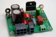
In addition to a well designed circuit and state-of-the-art board layout, the LM3886DR comes with a 30+ page design document that describes how the circuit works, how to assemble it, and how to use the board to build a complete amplifier. The design document contains over a dozen pictures illustrating the build process, including how to mount the LM3886 to the heat sink.
The project is also supported by a project set up with Mouser Electronics for easy ordering of parts. The bill-of-materials cost for the board is just shy of $27.
I have attached some build pictures and performance measurements. The measurements were performed using a regulated ±30 V power supply. Enjoy.
Thanks,
Tom
There are many LM3886 circuit boards on the market today, and let's face it, most of them are of dubious quality to say the least. Many kits don't come with instructions and some kits contain fake parts. It is therefore understandable that many people, in particular relative beginners, have a hard time telling the wheat from the chaff. My intent with the LM3886 Done Right is to relieve this anxiety by providing a LM3886 board that uses genuine parts and is fully optimized, well documented, well characterized, and well supported. In other words; Done Right.
The circuit is available for sale through my website: www.neurochrome.com
The full list of specifications is listed there as well. All specifications are based on measurements of the LM3886DR, not data sheet figures.
The LM3886DR contains all components needed for stability - even into significant capacitive load. In addition it features an RF filter on the input to eliminate RF and electromagnetic interference from switch arcing, WiFi, cell phones, etc.
The PCB is laid out uses elaborate pours and planes to ensure the lowest possible power supply impedance and ground impedance resulting in the best possible performance.
The LM3886DR actually beats the data sheet performance of the LM3886 on midrange THD+N!
In addition to a well designed circuit and state-of-the-art board layout, the LM3886DR comes with a 30+ page design document that describes how the circuit works, how to assemble it, and how to use the board to build a complete amplifier. The design document contains over a dozen pictures illustrating the build process, including how to mount the LM3886 to the heat sink.
The project is also supported by a project set up with Mouser Electronics for easy ordering of parts. The bill-of-materials cost for the board is just shy of $27.
I have attached some build pictures and performance measurements. The measurements were performed using a regulated ±30 V power supply. Enjoy.
Thanks,
Tom
Attachments
-
 LM3886DR_ASSY.jpg177.8 KB · Views: 2,803
 -
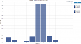
 LM3886DR Rev. 1.0_ Multi-Tone IMD (45 W, 8 ohm, AP 32-tone).PNG80.3 KB · Views: 425
 -
 LM3886DR Rev. 1.0_ IMD (DFD 18+19 kHz @ 1_1, 45 W, 8 ohm).PNG33 KB · Views: 343
 -
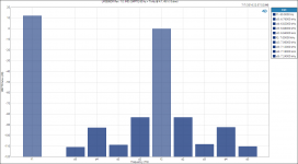 LM3886DR Rev. 1.0_ IMD (SMPTE 60 Hz + 7 kHz @ 4_1, 45 W, 8 ohm).png40.1 KB · Views: 358
 -
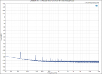 LM3886DR Rev. 1.0_ Residual Mains Hum (Power-86 + Antek AS-2222 Toroid).PNG48.3 KB · Views: 429
 -
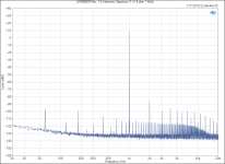 LM3886DR Rev. 1.0_ Harmonic Spectrum (1 W, 8 ohm, 1 kHz).PNG57.3 KB · Views: 463
 -
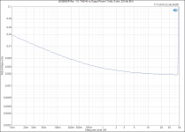 LM3886DR Rev. 1.0_ THD+N vs Output Power (1 kHz, 8 ohm, 22 kHz BW).PNG37.4 KB · Views: 2,443
 -
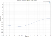 LM3886DR Rev. 1.0_ THD+N vs Frequency (45 W, 8 ohm, 80 kHz BW).png27.7 KB · Views: 2,462
 -
 LM3886DR Rev. 1.0_ Frequency Response (1 W, 8 ohm).png37.1 KB · Views: 2,587
 -
 LM3886DR_ASSY2.jpg168.7 KB · Views: 2,699
Last edited:
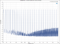
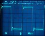
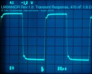
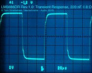
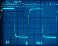
Attached plots shows the THD+N performance of the LM3886DR with a 4 Ω load.
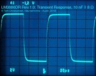
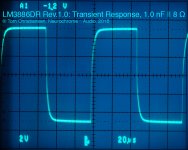
Also shown is the transient (step) response for various load capacitances. The ringing you see in the 1.0 µF || 8 Ω step response is actually the resonance between the output inductor and its dampening resistor. You can barely make out the onset of this resonance in the 220 nF || 8 Ω scope shot as well. As you can see, the LM3886DR is rock solid and completely stable, even with a large capacitive load.
Tom
Attachments
-
 LM3886DR Rev. 1.0_ THD+N vs Output Power (1 kHz, 4 ohm, 22 kHz BW).PNG42.9 KB · Views: 188
 -
 LM3886DR Rev. 1.0_ THD+N vs Frequency (80 W, 4 ohm, 80 kHz BW).PNG28.4 KB · Views: 323
 -
 LM3886DR_R1p0_Transient_1uF8R.jpg159.9 KB · Views: 257
 -
 LM3886DR_R1p0_Transient_470nF8R.jpg157.2 KB · Views: 210
 -
 LM3886DR_R1p0_Transient_220nF8R.jpg160.1 KB · Views: 181
 -
 LM3886DR_R1p0_Transient_100nF8R.jpg158.5 KB · Views: 186
 -
 LM3886DR_R1p0_Transient_47nF8R.jpg158.8 KB · Views: 163
 -
 LM3886DR_R1p0_Transient_10nF8R.jpg161.5 KB · Views: 196
 -
 LM3886DR_R1p0_Transient_1nF8R.jpg162.1 KB · Views: 232
 -
 LM3886DR_R1p0_Sine.jpg163.4 KB · Views: 234
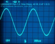
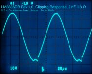
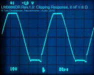
And finally the clipping response, both at the onset of clipping and hard into clipping. The scope shot shows the classic LM3886 rail sticking on the negative rail. Note that the LM3886DR shows no tendency to parasitic oscillation or buzz on overload and overload recovery.
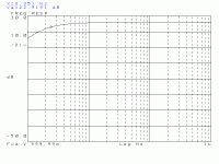
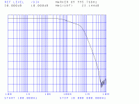
In addition to the frequency response plot shown in Post #1, I performed a frequency response measurement from 1 Hz to 1 kHz using an HP 3563A Dynamic Signal analyzer to determine the lower -3 dB frequency. I used an HP 3577A Network Analyzer to measure the frequency response from 100 Hz to 10 MHz for the upper -3 dB frequency and to characterize the performance of the RF input filter. The results are shown in the last two plots. The markers are placed at the -3 dB frequency (i.e. 3 dB down from the gain at 1 kHz).
Tom
Attachments
Last edited:
Tom,
Kudos.
And for the parsimonious, thrifty, penny-pinching DIY'ers out there that balk at the ($35/board + $27 parts) $62 cost to build one channel of this exquisite amplifier, please bark on some other thread or forum, please.
Goodbye fake Chinese eBay ripoffs and hello LM3886-DR!
Best,
Anand.
Kudos.
And for the parsimonious, thrifty, penny-pinching DIY'ers out there that balk at the ($35/board + $27 parts) $62 cost to build one channel of this exquisite amplifier, please bark on some other thread or forum, please.
Goodbye fake Chinese eBay ripoffs and hello LM3886-DR!
Best,
Anand.
Thank you! I did indeed keep the build budget in mind when I designed this amp. Including the power supply, connectors, heat sinks, chassis, etc., you're looking at $200 for a stereo build, assuming you build your own chassis and shop around a bit. That's really quite reasonable. If you already have suitable heat sinks, transformers, etc. you can reduce the cost considerably.
My business model is to deliver the best circuits out there. Circuits which are well designed, well tested, well characterized, and well documented. I deliver confidence. Confidence that builders, even beginners, can complete the build according to the instructions and end up with an amplifier that performs as well as indicated by the measurements.
The circuit is the result of my work to get to know the LM3886 rather intimately. I have come across everyone of its quirks in the design and prototyping of my Modulus-86 amp. The layout of the LM3886DR is the culmination of the advice I give on my Taming the LM3886 Pages and have dished out here on DIY Audio. I practice what I preach and I get good results. Thank you for noticing.")
Tom
My business model is to deliver the best circuits out there. Circuits which are well designed, well tested, well characterized, and well documented. I deliver confidence. Confidence that builders, even beginners, can complete the build according to the instructions and end up with an amplifier that performs as well as indicated by the measurements.
The circuit is the result of my work to get to know the LM3886 rather intimately. I have come across everyone of its quirks in the design and prototyping of my Modulus-86 amp. The layout of the LM3886DR is the culmination of the advice I give on my Taming the LM3886 Pages and have dished out here on DIY Audio. I practice what I preach and I get good results. Thank you for noticing.
Tom
What Anand said.
Thanks for another well-engineered kit, Tom! I've been admiring the Modulus-86 for some time, but consider it overkill for my needs. This might just fit the bill for a few of my bucket projects in the multi-way active speaker category
I plan to order a pair of bare boards when the Canada Post strike is settled.
I have two questions, one very relevant, the other academic:
1. Looking at the pic of the 3886-DR board on your website, one thing really jumped out at me. I've read all the threads on taming the 3886, optimizing a P-to-P 3886, etc., and the utmost importance of a short, low-inductance connection of Rf from pin 9 to pin 3. Illustrated at http://www.neurochrome.com/wp-content/uploads/2014/02/LM3886_Layout.png. It appears at first glance that the 3886-DR layout violates this cardinal rule in a big way. No argument about the exemplary measured performance of the 3886-DR, but I'd appreciate your comments on this. I'm sure you have good reasons, or my observation is faulty.
2. Bob Cordell has stated that (without going to the lengths of a Modulus-86 design effort) the LM3886 offers the best performance when operated in inverting mode, fed by an (high-quality) inverting op-amp. Have you ever tried this? Any comments?
Thank you, and thank you.
-Peter
What Anand said.
Thanks for another well-engineered kit, Tom! I've been admiring the Modulus-86 for some time, but consider it overkill for my needs. This might just fit the bill for a few of my bucket projects in the multi-way active speaker category
Awesome. Thank you.
I plan to order a pair of bare boards when the Canada Post strike is settled.
Well, Canada Post withdrew their 72-hour lockout notice (link). The workers can still go on strike, but they've previously said they'd rather negotiate. Trust me. I'm monitoring that situation rather closely.

Note the current introductory offer of $35/board is good until July 24. Christmas in July Intro Sale.
 I don't normally do sales.
1. Looking at the pic of the 3886-DR board on your website, one thing really jumped out at me. I've read all the threads on taming the 3886, optimizing a P-to-P 3886, etc., and the utmost importance of a short, low-inductance connection of Rf from pin 9 to pin 3.
It appears at first glance that the 3886-DR layout violates this cardinal rule in a big way.
I've learned quite a bit about the LM3886 since I wrote that part of the Taming series and have been wanting to rewrite some of the material and add new material for quite a while. What I write on the Stability page is fundamentally true, but the issue is much more complex so more context is needed. Note that the Thiele network isolates the load capacitance from the inductance in the feedback network. Thus, with a Thiele network in place, the layout requirements loosen up a bit.
The next thing to consider is which voltage you are trying to control. If you want the output voltage at Pin 3 of the LM3886 to be tightly controlled, then the layout I show on the Stability page is the best. However, with the Thiele network isolating the feedback inductance from the load capacitance, more feedback inductance (= trace length) can be afforded (within reason). This allows you to tap off the feedback point right where the output current enters the Thiele inductor. This means the voltage droop across the output pour and any THD developed due to the output connection will get attenuated by the loop gain of the LM3886. That's the best performance you can get and that's what I used in the LM3886DR.
2. Bob Cordell has stated that (without going to the lengths of a Modulus-86 design effort) the LM3886 offers the best performance when operated in inverting mode, fed by an (high-quality) inverting op-amp. Have you ever tried this? Any comments?
That's true. I show data here: LM3886 P2P vs PCB (with data) Post #36. Now you need to add an opamp driver. If you want the circuit to be non-inverting from input to output, the opamp driver needs to be inverting. Now you need a buffer to drive the inverting opamp driver. You also need to provide a regulated supply for the opamp. You go down that wormhole and suddenly you're a THAT1200 short of a Modulus-86, so why not just build one of those?
My goal with the LM3886DR is to provide a circuit that extracts the most out of the LM3886 while being relatively easy to assemble, thus, beginner-friendly and also being relatively easy on the wallet.
Tom
Last edited:
Thanks Tom!
... for the lucid and logical and between-the-lines explanations to both questions. How does a competent engineer get to have marketing chops, eh? It ain't fair.
Now I'll have to justify the budget for a pair of Modulus-86 to my better half as well... "We really need these for the front compression drivers, Honey, you know how they sounded with the tube amps you liked, before we downsized"
I'd like to offer another compliment, but it's meaningless without some background, so please forgive my rambling. PCB Art. And, appreciation of (parasitic) inductance.
Chapter 1: PCB Art:
Back in the late '70's-early'80's, I was regularly doing PCB artwork, as well as electronic design for professional sound and lighting products for live concert support. Signal-level stuff, not power. Back then, it involved multi-layer tape-ups, shoot a neg, shoot a pos, use a soldermask pad-master neg minus the blue overlay as a groundplane overlay with taped pad connections and sectioning, all pin-registered on a light table with a precision grid. All done with Red/Blue photo color separation for layers, multiple photo shoots, and overlays on mylar base. "Shoot a neg of this pos with a blue filter, and a pos with a red filter, and a pos of the blue, so I can divide the groundplane overlaid with the other neg...the red connects the pads, the blue divides the planes..."...
Fabrication drawings were done with Rapidograph ink pens and lettering templates on matte mylar on a vinyl-surface drafting board.
Interpret all dimensions and tolerances in accordance with ANSI Y14.5m...
When I sent my first set of negatives to a local PCB fab house back around 1979 (I used them up til 2004), I got a phone call from the owner of the company:
Him: "What CAD system are you using to produce these artworks? We need to know."
Me: "Uh, I'm using Bishop red and blue tape and black pads on a light table. X-Acto #16 blades only. XYZ Local industrial photo service."
Him: "We have work for you."
That lasted several years, but in the mid-80's I discovered OrCAD, around 1990-ish moved to OrCAD PCB386+, and have never looked back. (Until now)
Chapter 2: Appreciation of Parasitic Inductance
Later, I was principally involved in design of switchmode power supplies. Multi-Kw PFC regulators feeding buck regulators feeding bridge inverters with programmable output waveforms feeding arc lamps. When you're feeding 380V into a 500v rated MOSFET switching loop at 10's or 100's of amperes, you get to appreciate every nH. It's the "squared" part of I(squared)*L that bites. One also becomes painfully aware of ground return current patterns in the 4-layer mixed signal board that controls this monster.
OK, enough about me. None of this will be relevant to Golden Pinnae. The whole purpose of that storytelling was to help justify my opinion to the technically aware. I'm very critical of marginal PCB layout practice, signal routing, manufacturability, aesthetics, adherence to industry standards. It speaks nothing to my appreciation of listening to music, but facts don't lie.
IMO, Tom's LM3886 circuit boards are true Works of Art. Technically, and Aesthetically, on every level. I have no affiliation, just interest and admiration for competent engineering talent.
-Peter
... for the lucid and logical and between-the-lines explanations to both questions. How does a competent engineer get to have marketing chops, eh? It ain't fair.
Now I'll have to justify the budget for a pair of Modulus-86 to my better half as well... "We really need these for the front compression drivers, Honey, you know how they sounded with the tube amps you liked, before we downsized
" I'd like to offer another compliment, but it's meaningless without some background, so please forgive my rambling. PCB Art. And, appreciation of (parasitic) inductance.
Chapter 1: PCB Art:
Back in the late '70's-early'80's, I was regularly doing PCB artwork, as well as electronic design for professional sound and lighting products for live concert support. Signal-level stuff, not power. Back then, it involved multi-layer tape-ups, shoot a neg, shoot a pos, use a soldermask pad-master neg minus the blue overlay as a groundplane overlay with taped pad connections and sectioning, all pin-registered on a light table with a precision grid. All done with Red/Blue photo color separation for layers, multiple photo shoots, and overlays on mylar base. "Shoot a neg of this pos with a blue filter, and a pos with a red filter, and a pos of the blue, so I can divide the groundplane overlaid with the other neg...the red connects the pads, the blue divides the planes..."...
Fabrication drawings were done with Rapidograph ink pens and lettering templates on matte mylar on a vinyl-surface drafting board.
Interpret all dimensions and tolerances in accordance with ANSI Y14.5m...
When I sent my first set of negatives to a local PCB fab house back around 1979 (I used them up til 2004), I got a phone call from the owner of the company:
Him: "What CAD system are you using to produce these artworks? We need to know."
Me: "Uh, I'm using Bishop red and blue tape and black pads on a light table. X-Acto #16 blades only. XYZ Local industrial photo service."
Him: "We have work for you."
That lasted several years, but in the mid-80's I discovered OrCAD, around 1990-ish moved to OrCAD PCB386+, and have never looked back. (Until now
)Chapter 2: Appreciation of Parasitic Inductance
Later, I was principally involved in design of switchmode power supplies. Multi-Kw PFC regulators feeding buck regulators feeding bridge inverters with programmable output waveforms feeding arc lamps. When you're feeding 380V into a 500v rated MOSFET switching loop at 10's or 100's of amperes, you get to appreciate every nH. It's the "squared" part of I(squared)*L that bites. One also becomes painfully aware of ground return current patterns in the 4-layer mixed signal board that controls this monster.
OK, enough about me. None of this will be relevant to Golden Pinnae. The whole purpose of that storytelling was to help justify my opinion to the technically aware. I'm very critical of marginal PCB layout practice, signal routing, manufacturability, aesthetics, adherence to industry standards. It speaks nothing to my appreciation of listening to music, but facts don't lie.
IMO, Tom's LM3886 circuit boards are true Works of Art. Technically, and Aesthetically, on every level. I have no affiliation, just interest and admiration for competent engineering talent.
-Peter
Fabrication drawings were done with Rapidograph ink pens and lettering templates on matte mylar on a vinyl-surface drafting board.
[...]
When I sent my first set of negatives to a local PCB fab house back around 1979 (I used them up til 2004), I got a phone call from the owner of the company:
Him: "What CAD system are you using to produce these artworks? We need to know."
Me: "Uh, I'm using Bishop red and blue tape and black pads on a light table. X-Acto #16 blades only. XYZ Local industrial photo service."
I know people who worked on IC layouts like that. Black tape. Mylar sheets. Design rule check with a ruler. The design group I worked with in Santa Clara, CA still had the light table that they used to use for layout work.
That lasted several years, but in the mid-80's I discovered OrCAD, around 1990-ish moved to OrCAD PCB386+, and have never looked back. (Until now
OrCAD386 and OrCAD 4. I don't miss those. While the newer versions of OrCAD maintained some of the quirkiness of the old DOS-based tools, they're much nicer to work with.
Chapter 2: Appreciation of Parasitic Inductance
Later, I was principally involved in design of switchmode power supplies. Multi-Kw PFC regulators feeding buck regulators feeding bridge inverters with programmable output waveforms feeding arc lamps. When you're feeding 380V into a 500v rated MOSFET switching loop at 10's or 100's of amperes, you get to appreciate every nH. It's the "squared" part of I(squared)*L that bites.
Oof! Yes. I did some switch mode supply design in college. Obviously not at production level or the power levels you mention. Still enough to make me appreciate layout and device parasitics.
Taking my design skills to the IC world was another lesson in how the layout is the circuit.
IMO, Tom's LM3886 circuit boards are true Works of Art. Technically, and Aesthetically, on every level. I have no affiliation, just interest and admiration for competent engineering talent.
Thank you. I appreciate it.
Tom
It would be adequate for casual and most critical listening. If you really crank it, the SMPS-86 will run out of current on the peaks with 4 Ω drivers. If you want to be able to really crank it, I suggest running one 4 Ω driver per SMPS-86 and up to two 8 Ω drivers per SMPS-86.
Tom
Tom
Hi Tom,
Nice work, very pleased that I found your web page and analysis backed up
with simulation and measurements - very nice work.
I want to use an LM3886 for speaker measurements and perhaps other
measurements with a portable rig that I'm setting up.
I read your stability analysis with particular interest in Cc and you write:
"The degradation in phase/gain margin is primarily caused by Cc. According to the data sheet (pp. 8, 22), the purpose of Cc is to eliminate quasi oscillation caused by the pickup of EMI from the engagement of the SPiKe over-current protection. Cc is needed if the output impedance of the source driving the LM3886 is high and long signal traces are used. It follows that the quasi oscillation issue could just as well be addressed by lowering the source impedance or placing a resistor from the non-inverting input pin to ground on the LM3886. The EMI filter can then be placed on the non-inverting input of the LM3886, where it does not affect the phase margin."
If I'm reading you correctly it is better not to use Cc yet I see that you included it
as C5 in your layout.
I'm considering using larger input and feed back to ground caps to minimize
pass band phase shift for measurements.
The LM3886DR was done a few years after I wrote the stability pages. What's in the LM3886DR and its design doc is correct and the best practice. Please follow the LM3886DR design doc.
What is in the stability pages needs an update. The information is incomplete and I need to do a better job at putting it into context. Pardon the confusion.
The bandwidth of the LM3886DR is 2.4 Hz to 90 kHz. The 90 kHz is set by Cc and Cf combined. That corner is driven pretty hard by the LM3886 and the desire to keep its quasi-oscillation under control. The 2.4 Hz is set by the input cap. It causes a degree or two of phase shift at 20 Hz. That's not a concern as far as I know.
Tom
Thanks Tom,
Also your suggestion for 15R and 22nF on the Zobel is far off from the
data sheet value. Was the initial layout partly cause for the higher
value, did they change in the final layout?
Concerned that people reading here might just use the values you mention
in a design where they are not right for the layout.
You may want to check the design documentation. Specifically, items 9 and 30 on the BOM on page 27. You'll find that the values I specify for the LM3886DR are different from the 22nF/15Ω you mention above. I'm not sure where you got those values from.
I use a different resistor in the Thiele (L||R) network than shown in the data sheet to give better transient response.
I'm not sure what your concern is. The LM3886DR will perform according to its specifications when assembled according to the BOM on page 27 in the design documentation that you will receive when order my boards.
Tom
Here in the pictures from your P2P thread you show 10R and .33 nF in the schematic, and the comment on the P2P square wave states 15R and .22 nF you also mention these values in the text. I just thought that the thread was the development of this final design and want to understand what you did before buying one:
http://www.diyaudio.com/forums/chip-amps/252436-lm3886-pcb-vs-point-point-data.html
http://www.diyaudio.com/forums/chip-amps/252436-lm3886-pcb-vs-point-point-data.html
The LM3886 P2P vs PCB thread is from March 2014. It was part of the grounding investigations for the Modulus-86. The LM3886DR is from July 2016. It should be pretty obvious that a few things have settled in the meantime. Just because I used one value in a prototype circuit to investigate grounding in 2014 doesn't mean I use the same values in my production level circuit in 2016.
The LM3886DR combine the "Typical Application" and "AC Test #2" schematics from the LM3886 data sheet, applies all the tricks listed in the application section of the data sheet, applies a good layout (resulting in part from the investigations in the P2P vs PCB thread and my subsequent simulations), applies good decoupling, adds an RFI/EMI filter, and boxes all that up in an easy to assemble DIY project. I have run the full performance characterization suite on the LM3886DR. You can find the results on my website and in the first few posts of this thread.
Tom
Last edited:
- Home
- Vendor's Bazaar
- Neurochrome LM3886 Done Right - 45 W, 8 Ω, 0.002 % THD+N; 80 W, 4 Ω, 0.004 % THD+N